App-20
*2: If the processing overlaps those of the other CPUs in a multiple CPU system, the processing time increases
by a maximum of the following time.
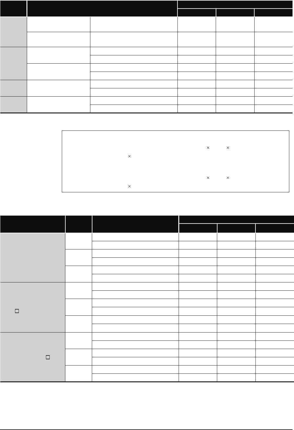
(6) Table of the time to be added when file register, module access device or link direct device is
used
Instruction
Name
Condition/Number of Points Processed
Processing Time (µs)
Q00JCPU Q00CPU Q01CPU
COM
*2
With auto refresh of CPU
shared memory
Refresh range: 2k words
(0.5k words assigned equally to all CPUs)
––
920 880
Without auto refresh of CPU
shared memory
–– ––
150 135
FROM
Read from CPU shared
memory of host CPU
n3 = 1
––
100 90
n3 = 320
––
440 420
Read from CPU shared
memory of another CPU
n3 = 1
––
110 105
n3 = 320
––
305 290
TO
Write to CPU shared memory
of host CPU
n3 = 1
––
100 95
n3 = 320
––
440 425
S.TO
Write to CPU shared memory
of host CPU
n4 = 1
––
205 195
n4 = 320
––
545 525
For a system having only the main base unit
(Instruction processing time increase) = 4 0.54 (number of points
processed) (number of other CPUs) (µs)
For a system including extension base units
(Instruction processing time increase) = 4 1.30 (number of points
processed) (number of other CPUs) (µs)
Instruction Name data
Device Specification
Location
Processing Time (µs)
Q00JCPU Q00CPU Q01CPU
File register (ZR)
Bit
Source
––
34 32
Destination
––
23 22
Word
Source
––
13 12
Destination
––
98
Double
word
Source
––
14 13
Destination
––
10 9
Module access device
(Un\G , U3En\G0 to G511)
Bit
Source
99
82 77
Destination
167
137 129
Word
Source
74
61 58
Destination
72
60 56
Double
word
Source
76
63 59
Destination
92
75 71
Link direct device (Jn\ )
Bit
Source
178
147 137
Destination
303
248 233
Word
Source
154
126 118
Destination
153
125 117
Double
word
Source
155
127 119
Destination
163
133 125


