2-57
1
2
4
4
2
6
7
8
2.5 Application Instructions
2.5.18 Other instructions
2.5.18 Other instructions
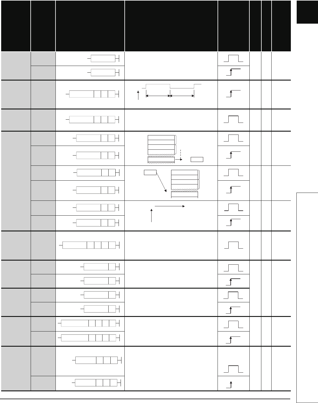
Table 2.35 Other Instructions
Category
Instruction Symbol
Symbol Processing Details
Execution
Condition
Number of Basic Steps
Subset
See for Description
WDT
reset
WDT
• Resets watchdog timer during sequence
program.
1 - 7-386
WDTP
Timing
clock
DUTY
4 - 7-388
Time check TIMCHK
• Turns ON device specified by (D) if
measured ON time of input condition is
longer than preset time continuously.
4 - 7-390
Direct read/
write
operations in
1-byte units
ZRRDB
3 - 7-391
ZRRDBP
ZRWRB
3 - 7-393
ZRWRBP
ADRSET
3 - 7-395
ADRSETP
Numerical
key input
from keyboard
KEY
• Takes in ASCII data for 8 points of input
unit designated by (S), converts to
hexadecimal value following device
number designated by (D1), and stores.
5 - 7-396
Batch save
of index
register
ZPUSH
• Saves the contents of index registers to a
location starting from the device
designated by (D).
2 - 7-400
ZPUSHP
Batch
recovery of
index register
ZPOP
• Reads the data stored in the location
starting from the device designated by
(D) to index registers.
ZPOPP
Batch write
operation to
E
2
PROM file
register
EROMWR
• Writes a batch of data to E
2
PROM file
register.
5 - 7-400
EROMWRP
Reading
module infor-
mation
UNIRD
• Reads the module information stored in
the area starting from the I/O No.
designated by n by the points designated
by n2, and stores it in the area starting
from the device designated by (D).
4-
UNIRDP
WDT
WDTP
DUTY n1 n2 D
n1 scans
SM420 to SM424, SM430 to SM434
(D)
n2 scans
TIMCHK S1 S2 D
ZRRDB n D
Lower 8 bits
(D)
Upper 8 bits
Lower 8 bits
Upper 8 bits
8 bits
0
1
2
3
n
ZR0
ZR1
ZRRDBP n D
ZRWRB n S
Lower 8 bits
(S)
Upper 8 bits
Lower 8 bits
Upper 8 bits
8 bits
0
1
2
3
n
ZR0
ZR1
ZRWRBP n S
ADRSET DS
(S) (D)
Indirect address of
designated device
Device name
ADRSETP SD
KEY D1 D2nS
ZPUSH D
ZPUSHP D
ZPOP D
ZPOPP D
EROMWR D1 D2nS
EROMWRP D1 D2nS
UNIRD n1 n2D
UNIRDP n1 n2D


