


106 www.xilinx.com SPI-4.2 Lite v4.3 User Guide
UG181 June 27, 2008
Chapter 5: Constraining the Core
R
through the Xilinx tools. The constraints generated in CORE Generator system are
provided as an example only and should be modified. You can modify these constraints to:
• Move the core placement to a different area
• Target a different device (other than the device package configuration)
See “Constraints Migration” for information on how to migrate the core to a different area
or device-package.
I/O Placement
With SPI-4.2 Lite, one has the flexibility to place the SPI-4.2 Lite I/Os according to
individual needs. You are not restricted to placing the I/Os in the bank options provided in
the GUI. You can define the placement of I/Os using 2 kinds of constraints: bank or pin-
lock constraints.
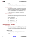
The following is an example of how to define I/O banks constraints:
• * INST "TDClk*" LOC = "Bank9"; #1 LVDS I/O pair
• * INST "TCtl*" LOC = "Bank9"; #1 LVDS I/O pair
• * INST "TDat*" LOC = "Bank9"; #16 LVDS I/O pairs
All SPI-4.2 Lite I/Os do not need to be in a single bank as given in the example. Ensure that
there are enough I/Os in the targeted bank (or banks) when using these constraints.
The following is an example of I/O pin lock constraint definitions:
• * NET "TDat_P(15)" LOC = "J23";
• * NET "TDat_P(14)" LOC = "K22";
• * NET "TDat_P(13)" LOC = "J26";
• * NET "TDat_P(12)" LOC = "L19";
• * NET "TDat_P(11)" LOC = "L21";
• * NET "TDat_P(10)" LOC = "K24";
To use these constraints, add the constraints and modify the pinout accordingly.
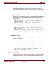
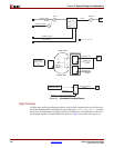
When using an area group to define the placement of the Source core, we recommended
placing the SPI-4.2 Lite pins (RCtl and RDat) in the same clock regions as the defined area
group. This is especially needed if regional clocking is used.
You have the same flexibility when placing SysClk and TSClk using the two constraints
above. However, there are some general guidelines when using different clocking options.
If regional clocking is used, SysClk must be placed on a clock-capable I/O pin that is in
the same clock region as the Sink core logic.
Using the example UCF file:
• * INST "SysClk" LOC = "Bank9";
If global clocking is used, SysClk must be placed on a pin that is connected to a global
clock buffer.
Using the example UCF file:
• * INST "SysClk*" LOC = "Bank4";
If regional clocking is used, TSClk must be placed on a clock capable I/O pin that is in the
same clock region as the source core logic.
Using the example UCF file: