


SPI-4.2 Lite v4.3 User Guide www.xilinx.com 17
UG181 June 27, 2008
R
Chapter 2
Core Architecture
This chapter describes the SPI-4.2 Lite core architecture and interface signals.
System Overview
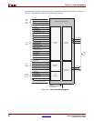
The SPI-4.2 Lite core is comprised of two separate cores that enable the transmission
(Source core) and reception (Sink core) of data.
• Sink Core. Receives data from the SPI-4.2 interface. It takes the 16-bit interface and
maps it to a 32-bit or 64-bit interface enabling the internal logic to run at a quarter of
the line rate.
• Source Core. Transmits data on the SPI-4.2 interface. Payload data written into the
core as 32-bit or 64-bit words (two or four 16-bit SPI-4.2 Lite words, respectively) is
mapped onto the 16-bit SPI-4.2 interface.
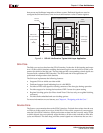
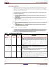
Figure 2-1 illustrates the interfaces of the SPI-4.2 Lite core and shows it in a typical link-
layer application.
In the link layer example, the SPI-4.2 interface connects an external physical-layer device to
a link-layer implemented in a Virtex™-4 FPGA. The user logic reads data from the Sink
core and writes data into the Source core. A standard FIFO interface is provided for this