


SPI-4.2 Lite v4.3 User Guide www.xilinx.com 65
UG181 June 27, 2008
Sink Core
R
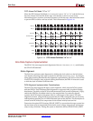
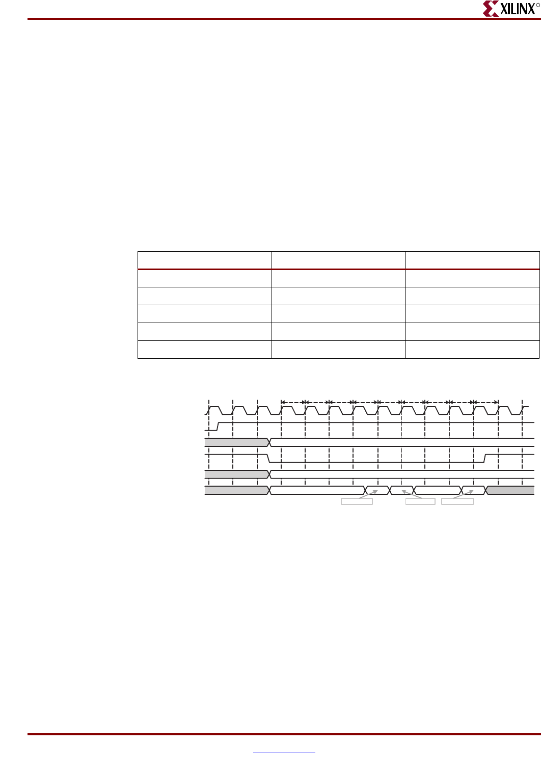
Sink Status FIFO Interface: Example 1
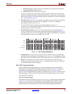
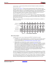
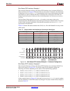
This example illustrates writing to the Status FIFO Interface for a 10-channel SPI-4.2 Lite
Sink core as shown in Figure 4-9. Because there are fewer than 17 channels, the Sink Status
Address bus (SnkStatAddr[3:0]) is permanently tied to zero. In this example, the mask
functionality is used to indicate that only 10 channels have valid status. The mask can
change from clock-cycle to clock-cycle, but in this illustration it is fixed (SnkStatMask=
0x03FF).
The Sink Status Write signal (SnkStatWr_n) is used to write status values to be
transmitted on the SPI-4.2 Interface in the order specified by the calendar buffer. The status
written in this example listed below. Note that the status data on SnkStat[31:0] is
represented in hexadecimal.
Table 4-4 shows the status written into SnkStat for each channel on every write
clock cycle.
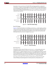
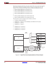
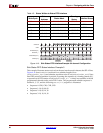
Sink Status FIFO Interface: Example 2
This example illustrates writing to the Status FIFO Interface for a 64-channel SPI-4.2 Lite
Sink core as shown in Figure 4-10. To write the status for 64 channels, address the
following four banks, depending on the status of the channel being updated:
• Bank 0: SnkStatAddr[3:0]= 0000, for channels 15 to 0
• Bank 1: SnkStatAddr[3:0]= 0001, for channels 31 to 16
• Bank 2: SnkStatAddr[3:0]= 0010, for channels 47 to 32
• Bank 3: SnkStatAddr[3:0]= 0011, for channels 63 to 48
In the example shown in Figure 4-10, the mask (SnkStatMask[15:0]) is used to update
only the channels for which FIFO status has changed. The status written in this example is
shown in Table 4-5.
Table 4-4: Status Written into SnkStat per Channel per Write Cycle
Write Cycle Starving Status Satisfied Status
0,1,2,3 CH 0-9 none
4 CH 1-9 CH 0
5 CH 1,2, 4-9 CH 0,3
6–7 CH 4-9 CH 0,1,2,3
8 CH 0 CH 1-9
Figure 4-9: Sink Status FIFO Interface Example 1: 10-channel Configuration
SnkStatClk
SnkStatMask[15:0]
SnkStatAddr[3:0]
SnkStat[31:0]
SnkEn
SnkStatWr_n
Write 0 Write 1 Write 2 Write 3 Write 4 Write 5 Write 6 Write 7 Write 8
BINARY
BINARY
HEX 0000.00AA0000.0000
0000.0011.1111.1111
0000
000A.AAA80000.00820000.0002