


SPI-4.2 Lite v4.3 User Guide www.xilinx.com 51
UG181 June 27, 2008
R
Chapter 4
Designing with the Core
This chapter contains general design guidelines, detailed descriptions about the behavior
of each interface, example waveforms, and implementation considerations. To design an
application using the SPI-4.2 Lite core, follow the guidelines provided in this chapter.
General Design Guidelines
This section describes the steps required to implement each feature of the SPI-4.2 Lite core
into a fully-functioning design integrated with user application logic. Remember that not
all designs will require all steps listed in this chapter.
We recommend you to follow the guidelines below for optimum results.
Know the Degree of Difficulty
A fully compliant SPI-4.2 Lite core is challenging to implement in any technology.
The degree of difficulty is significantly influenced by the following:
• Maximum system clock frequency
• Targeted device architecture
• Specific user application
All implementations require careful attention to system performance requirements.
Pipelining, placement constraints, and logic duplication are all methods you can use to
improve system performance.
Understand Signal Pipelining
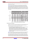
Due to the nature of packet protocols, it is important to understand that the SPI-4.2 Lite
Sink and Source cores have been pipelined to maximize performance. The 32- or 64-bit
data written into the Source core user interface takes several clock cycles before appearing
on the SPI-4.2 interface. This is due to the pipelining required to format the packet, create
control words, calculate DIP4, etc.
Similarly, SPI-4.2 packets that are received by the Sink core take several clock cycles before
appearing on the user interface. This is due to the pipelining required to convert the
streaming input bus to an aligned output with packet information, error signals, and so on.
The exact latency of the Sink and Source cores will vary based upon core configuration,
and is best determined through simulation.