


88 www.xilinx.com SPI-4.2 Lite v4.3 User Guide
UG181 June 27, 2008
Chapter 4: Designing with the Core
R
• ...
• Bank 14: SrcStatAddr[3:0]=14 for channels 239 to 224
• Bank 15: SrcStatAddr[3:0]=15 for channels 255 to 240
The status that is accessed is mapped to the 16-bit bus as follows (assuming SrcStatAddr
[3:0] = 0):
• SrcStat[1:0] => Channel 0, where SrcStat[1] is the MSB of the 2-bit status
• SrcStat[3:2] => Channel 1
• SrcStat[5:4] => Channel 2
• ...
• SrcStat[11:10] => Channel 13
• SrcStat[13:12] => Channel 14
• SrcStat[15:14] => Channel 15
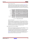
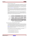
The operation of the Addressable Status FIFO interface is explained using three examples
described below and illustrated in Figure 4-30, Figure 4-31, and Figure 4-32.
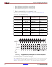
Addressable Status FIFO Interface: Example 1
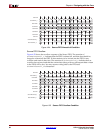
This example illustrates reading the Status FIFO Interface for a 4-channel Source core, as
shown in Figure 4-30. As there are fewer than 17 channels, the Source Status Address bus
(SrcStatAddr[3:0]) is permanently tied to zero. The Source Status address
(SrcStatAddr[3:0]) causes the Source Status data bus (SrcStat[31:0]) to be
updated on the next clock cycle. Both buses use the user-selected clock domain
(SrcStatClk), which can be tied to the SPI-4.2 Interface clock domain (TSClk_GP).
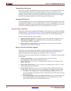
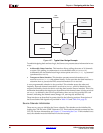
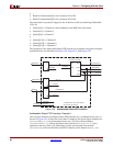
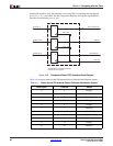
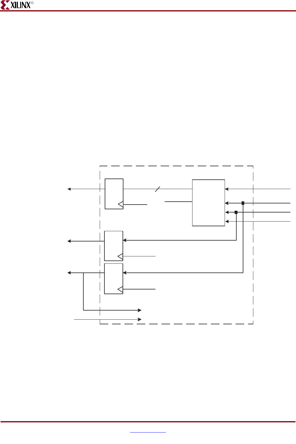
Figure 4-29: Addressable Status FIFO Interface
Q D
SrcStatClk
WData
WAddr
WEN
WCLK
SrcStatClk SrcStatClk
Q D
TSClk_GP
FIFO Status Cyclic Buffer
(Dual Port LUT RAM)
Q D
TSClk_GP
RData
RAddr
SrcStatAddr
SrcStatAddr
1
FifoWrAddress is the channel address
retrieved from the Calendar.
32
Write_En
FifoWrAddress
TStat_Delayed[1:0]
TSClk_GP
Write_En
FifoWrAddress
1
SrcStat[31:0]
SrcStatCh
SrcStatChValid