


108 www.xilinx.com SPI-4.2 Lite v4.3 User Guide
UG181 June 27, 2008
Chapter 5: Constraining the Core
R
Timing Ignore Constraints
If Source core static configuration signals are driven statically from a register, apply the
timing ignore attributes (TIG) to the static configuration signals to create proper timing
ignore paths. If these are driven statically from a wrapper file, then the TIG is not needed.
In the example UCF, these constraints are commented out. Uncomment these constraints in
your design.
• NET "SrcAFThresAssert(*)" TIG;
• NET "SrcAFThresNegate(*)" TIG;
• NET "DataMaxT(*)”;
• NET "AlphaData(*)”;
• NET "SrcBurstLen(*)”;
• NET "NumDip2Errors(*)”;
• NET "NumDip2Matches(*)”;
User Constraints
In certain cases, you may need to add additional constraints to cover other logic
implemented in your design. While the UCF file provided with the core is designed to
completely constrain the Xilinx SPI-4.2 Lite core, it may not adequately constrain user-
implemented logic interfaced to the core.
Constraints Migration
The example UCF file provided with the core must be modified to migrate the core to a
different area or target device.
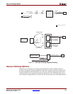
The examples in this section indicate the changes necessary to migrate the Sink and Source
cores to user-defined locations on a XC4VLX40-FF1148 Virtex-4 part by modifying the
example UCF that targets XC4LX25-FF1148. The static alignment example shows the
migration of the Sink and Source cores to the south-west region of the part (banks 11 and
8).
New Target Region or Device Package
When selecting a new target region or device package, first verify that the new region has
enough resources required for the generated core. Resources that need to be taken into
considerations are:
• Block RAMs
• I/O Pins (in targeted I/O banks)
• Logic cells
• Clocking resources: DCM, regional and global buffers
Below are some typical region selections within a device.
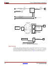
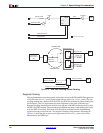
• Source Core: One clock region on the same side of the device, east or west.
• Sink Core (static): One clock region on the same side of the device.
The east side is the side of the device with even numbered I/O banks: 6, 8, 10, and so on.
The west side is the side of the device with odd numbered I/O banks: 5, 7, 9, and so on.