


70 www.xilinx.com SPI-4.2 Lite v4.3 User Guide
UG181 June 27, 2008
Chapter 4: Designing with the Core
R
setting has the added advantage of providing a benchmark of the system margin, based on
the UI (unit interval or bit time).
System Margin (ps) = UI(ps) * (working phase shift range/128)
Xilinx does not recommend that a single DCM PHASE_SHIFT value will be effective
across all hardware platforms. Xilinx also does not recommend that you attempt to
determine the PHASE_SHIFT setting empirically. In addition to the clock-to-data phase
relationship, other factors such as package flight time (package skew) and clock routing
delays (internal to the device) affect the clock-data relationship at the sample point (in the
IOB) and are difficult to characterize.
The optimal PHASE_SHIFT setting should be investigated during hardware integration
and debugging. Note that the phase shift setting provided with the SPI-4.2 Lite core in the
constraints file is only a place holder. This default setting has changed over various SPI-4.2
Lite releases to account for changes to the DCM DESKEW ADJUST attribute. For further
information on how to find the ideal phase shift value for your system, see the Xilinx SPI-
4.2 solution record 16112
.
Note:
This alignment method can be used only with global clock distribution.
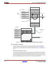
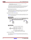
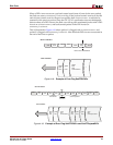
ISERDES Alignment Implementation Considerations (Virtex-4 and Virtex-5 only)
Static alignment can be performed using the IDELAY function of the Virtex-4 and Virtex-5
device ISERDES for regional clocking distribution. The ability of the IDELAY function to
delay its input by small increments (75ps), enables the internal RDClk to be shifted relative
to the sampled data. For statically aligned systems, the delay chain length is a critical path
of the system. The static alignment solution assumes that the PCB is designed with precise
delay and impedance matching for all LVDS differential pairs of the data bus. In this case,
the primary alignment mechanism is time shifting the internal RDClk relative to the data
bits using the IDELAY function.
you must determine the optimal delay in the ISERDES (IOBDELAY) to ensure that the
target system will have the maximum system margin and performance across voltage,
temperature, and process (chip to chip) variations. Xilinx does not recommend a single
IOBDELAY value that will be effective across all hardware platforms. Xilinx also does not
recommend that you attempt to determine the IOBDELAY setting empirically. In addition
to the clock-to-data phase relationship, other factors such as package flight time (package
skew) and clock routing delays (internal to the device) affect the clock data relationship at
the sample point (in the IOB) and are difficult to characterize. The optimal IOBDELAY
setting should be investigated during hardware integration and debugging. Note that the
IOBDELAY setting provided with the SPI-4.2 Lite core in the constraints file is only a place
holder.
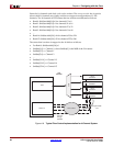
An example of this implementation is available through the GUI using the Sink core in user
clocking mode with regional clocking distribution.
Synchronization and Start-up
After the sink core has been initialized, as described in the “Initializing the SPI-4.2 Lite
Core,” it has to be synchronized before data and status can be received and transmitted.