


122 www.xilinx.com SPI-4.2 Lite v4.3 User Guide
UG181 June 27, 2008
Chapter 6: Special Design Considerations
R
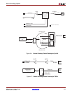
For each core constraints, the instance name in the UCF file must be modified to match the
instance names in the top-level RTL design. For the timing and I/O pin location
constraints, change the names to match the I/O ports declared in the top-level design as
shown in the examples below.
• TNMs and TIMESPECs:
Net “First_RDClk_P” TNM_NET = “First_RDClk_P”;
TIMESPEC “TS_First_RDClk_P” = PERIOD “First_RDClk_P” 100 MHz
HIGH 50%;
• I/O pins location:
INST “First_RDat*” LOC = BANK5”;
INST “First_RCtl” LOC = “BANK5”;
INST “First_RDClk” LOC = “BANK3 “;
INST “First_TDat*” LOC = “BANK9”;
INST “First_TCtl” LOC = “BANK9”;
See Chapter 5, “Constraining the Core” for details on how to place the Area Group, and IO
Bank components.
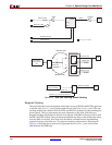
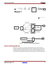
Clocking Considerations
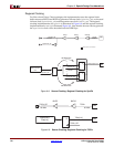
If the reference clock (SysClk) can be shared among different Source cores, we
recommend that Source cores with slave clocking be used in the design with the external
clocking module (pl4_lite_src_clk.v/vhd). For Virtex-4 or Virtex-5 FPGA designs, the SPI-
4.2 Source Status FIFO Clocks (TSClk) can be implemented using regional clock buffer
resources to further reduce the number of global clocks and DCMs used in the design.
The user can also use a single Source core in master clocking mode with global clock option
and use the clock outputs (SysClk180_GP and SysClk0_GP) of this core to drive the
other Source cores in slave clocking mode.
For example:
first_pl4_lite_src_top0 : pl4_lite_src_top1 --- Master clocking
mode
port map (
.........
SysClk180_GP => SysClk180_GP ;
SysClk0_GP => SysClk0_GP;
...........
);
second_pl4_lite_src_top0 : pl4_lite_src_top2 --- Slave clocking
mode
port map (
............
SysClkDiv_GBSLV => SysClk180_GP;
SysClk0_GBSLV => SysClk0_GP;