


SPI-4.2 Lite v4.3 User Guide www.xilinx.com 79
UG181 June 27, 2008
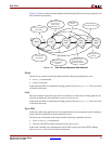
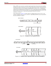
Source Core
R
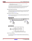
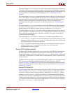
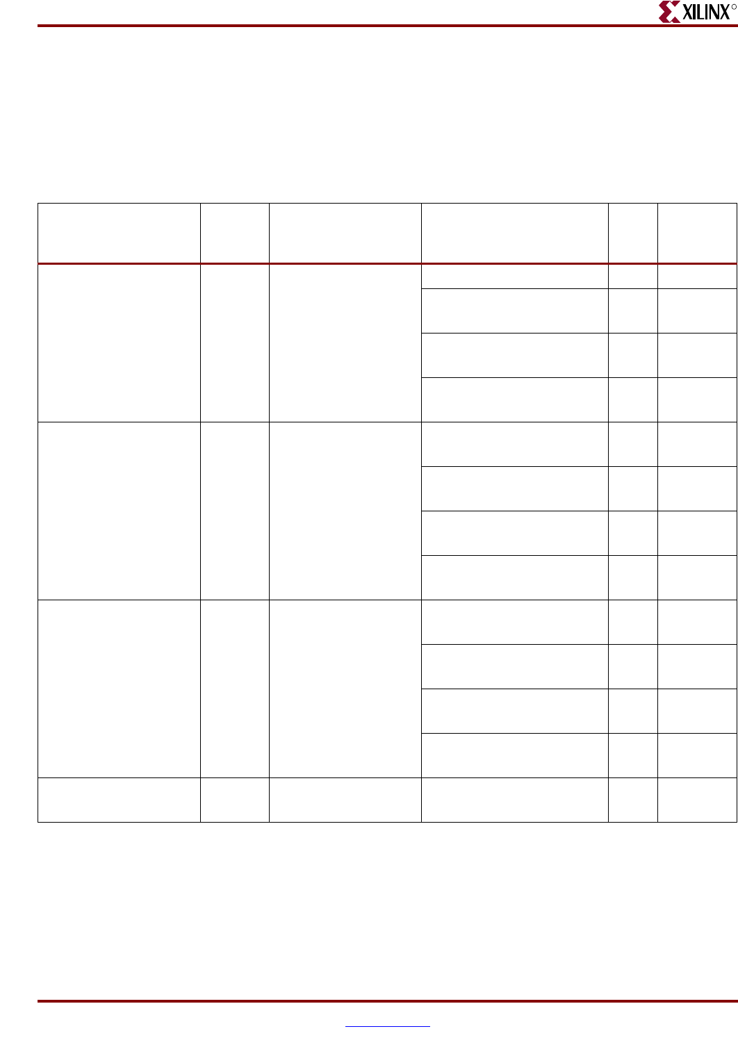
64-bit words from the Source FIFO are transmitted on the SPI-4.2 data bus. The DIP-4
parity depends on this control word and any proceeding transfer; therefore, it is left as
“pppp” (shown in the 13th TDClk clock cycle).
Following this example are two tables showing the mapping between the packet status
signals on the user interface and SPI-4.2 control words for a 32-bit user interface (Table 4-7)
and for a 64-bit user interface (Table 4-8).
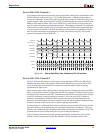
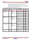
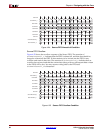
Table 4-6: Example of Formatting Source FIFO Data for a 64-bit User Interface
Data Written to the
Source FIFO
(SrcFFData[63:0])
SrcFFClk
Cycle
FIFO Control Bit
Data Transmitted on the
SPI-4.2 Interface
(TDat [15:0])
TCtl
TDClk
cycle
SrcFFData[63:0] =
[F1E2.D3C4.B5A6.9F8E]
1
SrcFFSOP = 1
SrcFFEOP = 0
SrcFFMOD = 000
SrcFFAddr = 0000.0010
SrcFFErr = 0
N/A N/A n
SOP
b:[1001.0000.0010.pppp]
1n+1
SPI-4.2 Lite Word 0 (P0)
F1E2
0n+2
SPI-4.2 Lite Word 1 (P1)
D3C4
0n+3
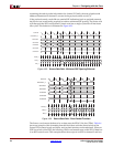
SrcFFData[63:0] =
[1F2E.3D4C.5B6A.F9E8]
2
SrcFFSOP= 0
SrcFFEOP = 0
SrcFFMOD = 000
SrcFFAddr = 0000.0010
SrcFFErr = 0
SPI-4.2 Lite Word 2 (P2)
B5A6
0n+4
SPI-4.2 Lite Word 3 (P3)
9F8E
0n+5
SPI-4.2 Lite Word 4 (P4)
1F2E
0n+6
SPI-4.2 Lite Word 5 (P5)
3D4C
0n+7
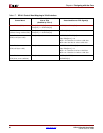
SrcFFData[63:0]
[ABCD.1200.0000.0000]
3
SrcFFSOP= 0
SrcFFEOP=1
SrcFFMOD = 011
SrcFFAddr = 0000.0010
SrcFFErr = 0
SPI-4.2 Lite Word 6 (P6)
5B6A
0n+8
SPI-4.2 Lite Word 7 (P7)
F9E8
0n+9
SPI-4.2 Lite Word 8 (P8)
ABCD
0n+10
SPI-4.2 Lite Word 9 (P9)
1200
0n+11
4
EOP / MOD
b:[0110.0000.0010.pppp]
1n+12