


SPI-4.2 Lite v4.3 User Guide www.xilinx.com 109
UG181 June 27, 2008
Constraints Migration
R
If the target region or device does not contain enough resources, this will result in tool
errors; not due to portability issues but resource issues.
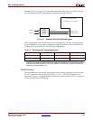
Modifying the UCF File
Once the target region is selected, the UCF file must be modified. While modifying the
constraints, ensure that changes are within the specifications described by the Sink and
Source core required constraints.
Note:
The use of optional constraints is up to user discretion.
Following are the UCF modifications:
Target Device
Change CONFIG_PART constraint to a desired device.
Sink Core
Specify pin placements for the SPI-4.2 Lite interface I/Os (RCtl* and RDat*). If regional
clocking is used, the I/Os must be constrained to pins that coincide with the clock regions
of the Sink core. If I/O bank constraints are used, verify that the targeted bank can
accommodate the total LVDS I/O pairs.
In the following example, Bank 8 must contain at least 17 LVDS I/O pairs:
• INST "RCtl*" LOC = "Bank8"; # 1 LVDS I/O pair
• INST "RDat*" LOC = "Bank8"; #16 LVDS I/O pairs
Specify pin placement for RDClk I/O. See “Placement Constraints,” page 102 for
information on placement constraints. For example:
INST "RDClk*" LOC = "Bank4";
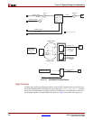
Specify an area group constraint if regional clocking is used. In the example UCF file, area
group "AG_pl4_lite_snk" is defined as one adjacent clock region on the same side of the
device.
For example:
AREA_GROUP "AG_pl4_lite_snk" RANGE = CLOCKREGION_X1Y0;
Place the IDELAYCTRL component in the same clock region as the core. For example:
• INST "<sink_instance_name>/rdclk_idelctl” = IDELAYCTRL_X1Y0;
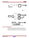
Source Core
Specify pin placement for "SysClk" I/O. See “Placement Constraints,” page 105. For
example:
INST "SysClk*" LOC = "Bank 4";
Specify pin placements for the SPI-4.2 Lite interface I/Os (TDClk*, TDat* and TCtl*). If
regional clocking is used, the I/Os must be constrained to pins that coincide with the clock
regions of the Source core. If I/O bank constraints are used, verify that the targeted bank
can accommodate the total LVDS I/O pairs.
In the following example, Bank 7 contains at least 18 LVDS I/O pairs:
• INST "TDClk*" LOC = "Bank7"; # 1 LVDS I/O pair