


90 www.xilinx.com SPI-4.2 Lite v4.3 User Guide
UG181 June 27, 2008
Chapter 4: Designing with the Core
R
• Bank 1: SrcStatAddr[3:0]= 0001, for channels 31 to 16
• Bank 2: SrcStatAddr[3:0]= 0010, for channels 47 to 32
• Bank 3: SrcStatAddr[3:0]= 0011, for channels 63 to 48
• ...
• Bank 15: SrcStatAddr[3:0]= 1111, for channels 255 to 240
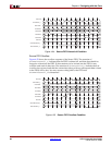
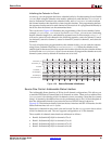
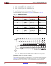
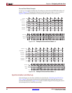
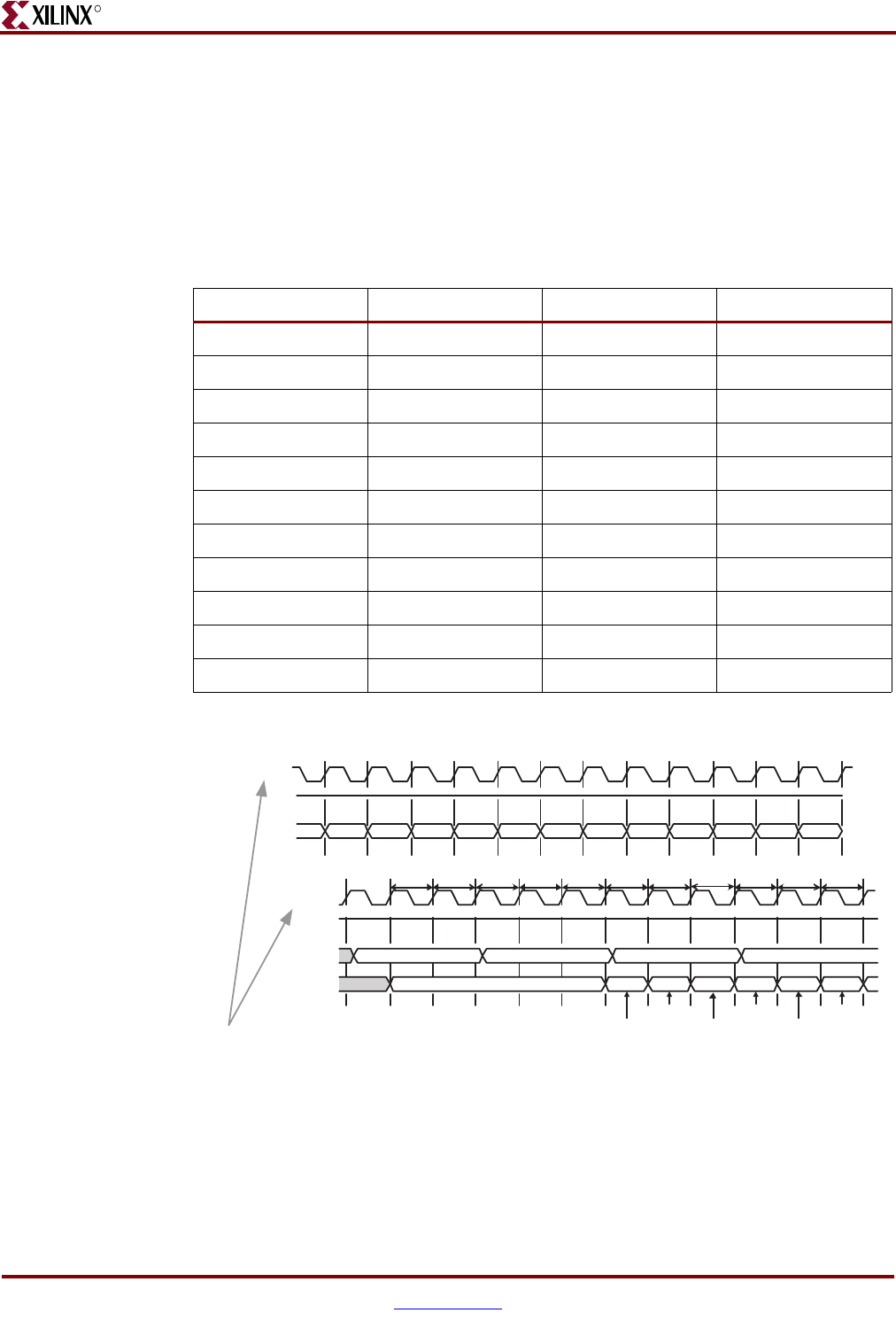
The status read in the example shown in Figure 4-31 is summarized in Table 4-10.
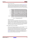
Addressable Status FIFO Interface: Example 3
This example illustrates status received on the SPI-4.2 bus and written to the user interface
(Figure 4-32). The calendar length is seventeen (SrcCalendar_Len=16) and calendar
repetition value is one (SrcCalendar_M=0). This illustrates a system in which the
Table 4-10: Status Read Summary
Read Cycle Status Address Starving Status Satisfied Status
0 Bank 15 CH 240–255 None
1 Bank 15 CH 240–255 None
2 Bank 15 CH 240–255 None
3 Bank 0 CH 0–15 None
4 Bank 0 CH 0–15 None
5 Bank 0 CH 1–15 CH 0
6 Bank 15 CH 242–255 CH 240–241
7 Bank 15 CH 243–255 CH 240–242
8 Bank 15 CH 241–254 CH 255
9 Bank 0 CH 0–13 CH 14–15
10 Bank 0 CH 0–12 CH 13–15
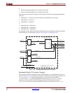
Figure 4-31: Addressable Status FIFO Interface: 256-channel configuration
0x00000002
0x0000000A
0x0000002A
0x80000000
0xA0000000
0xA8000000
Independent
Clock
Domains
SrcStatCh[7:0]
SrcStatValid
CH240 CH241 CH242 CH15 CH14 CH13 CH240 CH241 CH242 CH15 CH14 CH13
TSClk
SrcStatClk
SrcStatAddr[3:0]
1111 0000 1111
SrcStat[31:0]
SrcEn
0000
0x00000000
Read 0 Read 1 Read 2 Read 3 Read 4 Read 5 Read 6
Read 7
Read 8 Read 9 Read 10