


SPI-4.2 Lite v4.3 User Guide www.xilinx.com 21
UG181 June 27, 2008
Sink Core Interfaces
R
Sink SPI-4.2 Interface
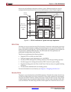
The SPI-4.2 interface uses LVDS I/O buffers to receive 16-bit data words. The 16-bit data
words received on the SPI-4.2 interface are combined into 32-bit or 64-bit data words by the
SPI-4.2 Lite core, which allows the user interface to run at a half (32-bit interface) or quarter
(64-bit interface) of the data rate. For example, for a 200 Mbps data rate and a 32-bit
interface, you can read data from the Sink core at 100 MHz, and if a 64-bit interface is used,
you can read data from the Sink core at 50 MHz and maintain the same data rate.
The resulting data words are written into an asynchronous FIFO. The received 16-bit
control words are stored out of band in the FIFO, along with the corresponding data word.
The received control words that are not idle or training words can contain the information
listed below:
• Start or continuation of the following packet
• Link address of the following packet
• End of the preceding packet
• Number of valid bytes in the last word of the preceding packet
• Error conditions in the preceding packet
In addition to receiving 16-bit data words, the SPI-4.2 interface also sends flow control data
at 1/4 rate (or 1/8 rate) of its data interface. The 32-bit status (2-bit status for each channel)
from the user interface is processed and formatted by the SPI-4.2 Lite core to be transmitted
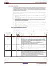
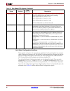
on RStat. Table 2-1 defines the Sink SPI-4.2 interface signals.
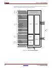
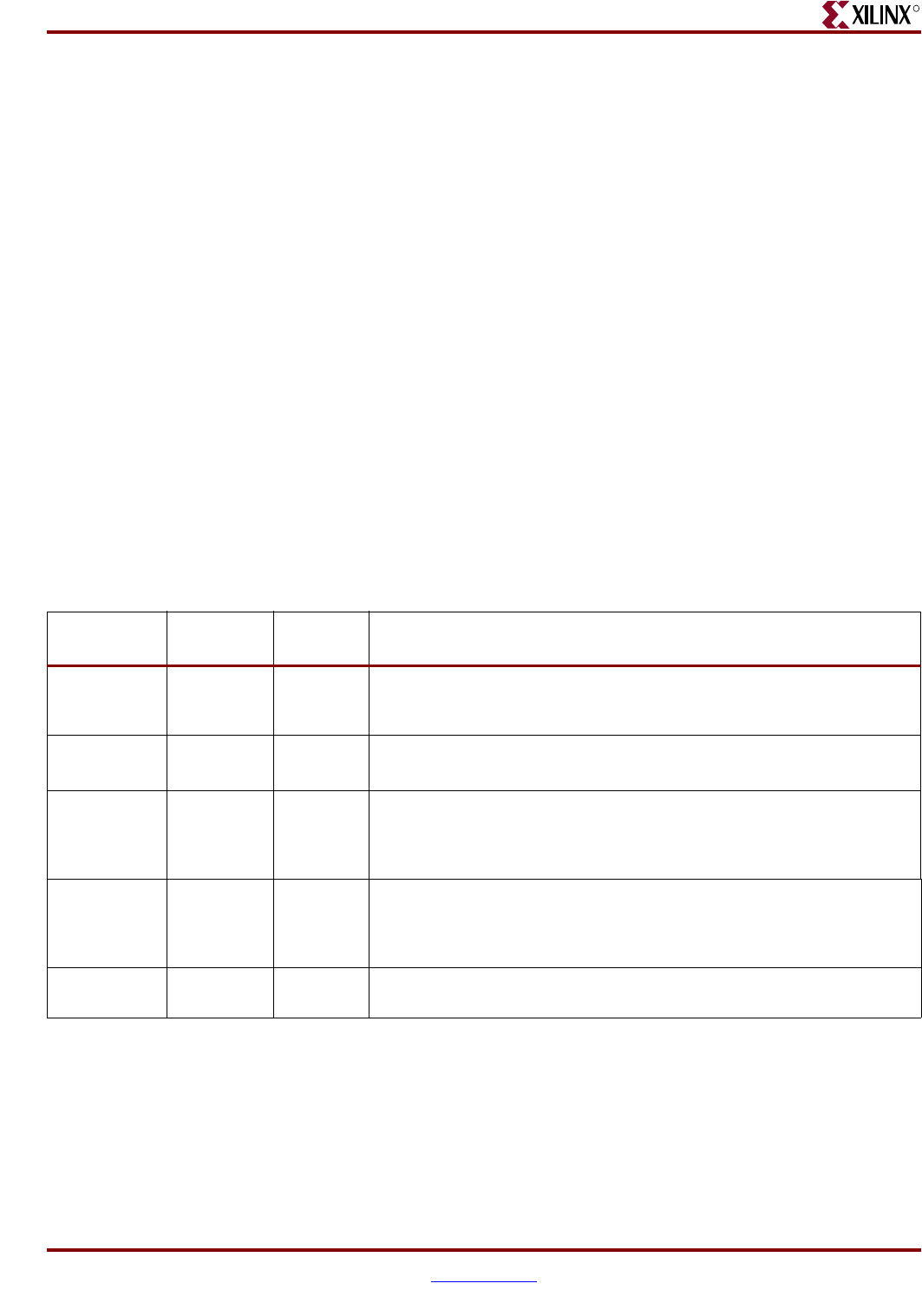
Table 2-1: Sink SPI-4.2 Interface Signals
Name Direction
Clock
Domain
Description
RDClk_P
RDClk_N
Input n/a SPI-4.2 Receive Data Clock (LVDS): Source synchronous clock received with
RDat and RCtl. The rising and falling edges of this clock (DDR) are used to
clock RDat and RCtl.
RDat_P[15:0]
RDat_N[15:0]
Input RDClk SPI-4.2 Receive Data Bus (LVDS): The 16-bit data bus used to receive SPI-4.2
data and control information.
RCtl_P
RCtl_N
Input RDClk SPI-4.2 Receive Control (LVDS): Signal that indicates whether data or control
information is present on the RDat bus. When
RCtl is deasserted, data is
present on RDat. When RCtl is asserted, control information is present on
RDat.
RSClk Output n/a SPI-4.2 Receive Status Clock: Source synchronous clock transmitted with
RStat at 1/2 or 1/4 rate of the RDClk. The rate of the status clock is controlled
by the static configuration signal RSClkDiv. You can select this signal to be
transmitted as LVTTL or LVDS.
RStat[1:0] Output RSClk SPI-4.2 Receive FIFO Status: FlFO Status Channel flow control interface. You
can select this bus to be transmitted as LVTTL or LVDS.