


SPI-4.2 Lite v4.3 User Guide www.xilinx.com 31
UG181 June 27, 2008
Source Core Interfaces
R
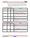
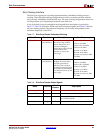
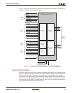
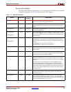
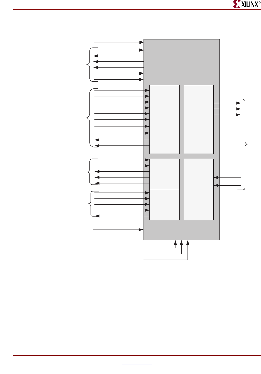
Figure 2-3 illustrates the functional modules and signals in each interface—all signals are
defined in sections following this illustration.
Source SPI-4.2 Interface
The SPI-4.2 interface uses LVDS I/O buffers to transmit 16-bit data words. The data words
received on the User Interface and the out-of-band control words are multiplexed onto the
SPI-4.2 Lite 16-bit databus. The source core supports a 32-bit and 64-bit user interface,
which allows it to run at a half (32-bit interface) or quarter (64-bit interface) of the data rate.
For example, for a 200 Mbps SPI-4.2 data rate and a 32-bit interface, you can write data into
the Source core at 100 MHz. If a 64-bit interface is used, you can write data into the Source
core at 50 MHz and maintain the same data rate.
Figure 2-3: Source Core Block Diagram and I/O Interface Signals
SPI-4.2 Lite Source Core
Control
and Status
Interface
Source Data
Transmit
Source Data
FIFO
Reset_n
SPI4.2
Source
Interface
FIFO
Interface
FIFO
Status
Interface
Calendar
Control
Interface
Source Status
Registers
Source
Calendar
Source Status
Receive
SrcFifoReset_n
SrcTriStateEn
TDClk
TDat[15:0]
TSClk
TStat[1:0]
TCtl
SysClk
SrcOof
SrcDIP2Err
SrcEn
TrainingRequest
IdleRequest
SrcPatternErr
SrcFFClk
SrcFFWrEn_n
SrcFFAddr[7:0]
SrcFFData[63:0] or [31:0]
SrcFFMod[2:0] or [1:0]
SrcFFSOP
SrcFFErr
SrcFFEOP
SrcFFAlmostFull_n
SrcFFOverflow_n
SrcStat[31:0]
SrcCalClk
SrcCalWrEn_n
SrcCalAddr[8:0]
SrcCalData[7:0]
Static Configuration Signals
SrcStatClk
SrcCalDataOut[7:0]
SrcStatAddr[3:0]
SrcStatCh[7:0]
SrcStatChValid