


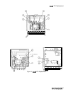
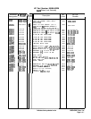

A6A9
A6A9
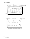
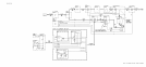
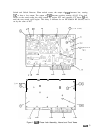
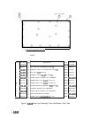
Phase Lock, Circuit Description
The A6A9 Phase Lock has three major functions:
1. To provide a stable -10.0
dBm,
100 MHz calibrator signal to the RF Section front panel.
2. To provide a 300 MHz local oscillator to the A6A3 Last Converter assembly.
3. To phase-lock the 3.3 GHz second local oscillator in the A6A4 Second Converter assembly
to the 33rd harmonic of the 100 MHz reference signal produced by the A7A2 100 MHz
VCXO assembly. This 3.3 GHz phase lock loop is called the Heterodyne Loop.
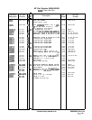
100 MHz Buffer Amplifier
@
The 100 MHz buffer amplifier
Ql
amplifies the reference signal from the A7A2 100 MHz
VCXO assembly. Low pass matching network,
Ll
and C4, provides a
5Ofl
input impedance.
Transformer
Tl
acts as a power divider, supplying the 100 MHz signal to both the Driver
circuit and the Phase Lock circuit.
Driver
@
Transistor Q2 amplifies the 100 MHz from the 100 MHz Buffer Amplifier. Power divider T2
drives both the 100 MHz Calibrator and the 300 MHz LO circuit.
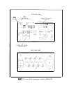
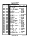
100 MHz Calibrator
@
The Calibrator circuit consists of a differential amplifier, Q3A and Q3B, followed by a low
pass filter. Low pass filters C19, L8, C20,
L9,
and C22, reduce higher order harmonics on the
front panel calibrator output. Potentiometer
Rll
and factory-select resistor RlO set the gain
of Q3.
Tripler
@
With the 100 MHz input from the Driver circuit, the Tripler circuit produces a 300 MHz
output at approximately
+6
dBm.
Inductor
LlO
and C24 are used for impedance matching.
The output tank circuit, formed by
Lll
and the output capacitance of transistor Q4, resonates
at 300 MHz. Capacitor C29 adjusts the loading of the stage and couples the output to the
Power Amplifier.
A6A9
1