


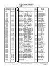
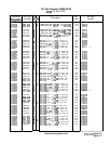
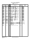
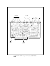

A7A2
A7A2 100 MHz Voltage-Controlled Crystal Oscillator (VCXO),
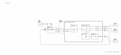
Circuit Description
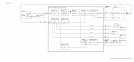
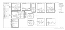
A7A2 consists of a 100 MHz voltage-controlled crystal oscillator, buffer amplifiers, and a
frequency quadrupler. In conjunction with
A7Al
Reference Phase Detector, it forms the
reference phase-lock loop. Outputs of 100 MHz and 400 MHz are used as frequency references
by other assemblies in the instrument.
100 MHz Oscillator
@
Q5 functions as a common-base amplifier with feedback to form an oscillator. The
feedback includes the 100 MHz crystal
Yl
and varactor CR1 which are the principal
frequency-determining components. CR1 is tuned by the output of
A7Al
and can vary the
frequency by approximately
fl
kHz. The amplitude of the oscillations is limited by CR3 and
CR4.
TPl
is accessible from the top cover; the voltage should be near -8 V dc for proper
operation. The voltage is adjusted by tuning the oscillator with C4.
100 MHz Buffer Amplifier
@
QS,
Q7,
QS,
Q9,
and
Qll
form a series of 100 MHz amplifiers. They buffer the 100 MHz
outputs from each other as well as from the oscillator.
Quadrupler
@
100 MHz from Q7 in
@J
is applied to T3. The secondary of T3 is connected to Q3 and Q4 to
form a full-wave rectifier. Positive half cycles of 100 MHz to T3 turn on Q3 while negative
half cycles turn on Q4. The collectors are connected together to sum the currents and produce
even harmonics of 100 MHz. The output is tuned to 400 MHz by C3 and
LlO
to select
400
MHz.
400 MHz Amplifier
@
Ql
and Q2 are two common-emitter tuned amplifier stages which amplify 400 MHz and filter
undesired harmonics of 100 MHz. R67, R68, and R69 form a pad which is selected to give
-10
dBm
f2
dB output at 400 MHz.
A7A2
1