


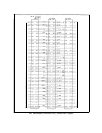
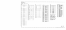
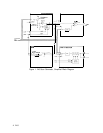

Ramp
Control
Logic
0,
Switch
Driver
@,
Ramp
Reset
Switch
@I,
and
Ramp Reset
Amplifier
@
The sweep ramp is formed by alternately charging and discharging Cl, according to the
following cycle.
Control line HSWP resets the sweep (High = Sweeping). When HSWP goes low (determined
by IF-Display Section), LHOLD (U5C pin 8)
g
oes low, turning on
CRl.
When CR1 is on,
charging current bypasses ramping capacitor Cl and instead passes to ground via
CRl.
Ramping capacitor Cl stops charging.
Ramping capacitor Cl holds its charge until LANR, from Front-Panel Interface Assembly
A12, goes low (Low = Analog Reset). When LANR goes low, LHOLD goes high, turning
CR1 off, removing the current bypass for ramping capacitor Cl. RESET/GO (U5D pin 11)
also goes high when LANR goes low, which turns
Q9
off. Q7 and Q6 then turn on, providing
a discharge path for Cl through Ramp Reset Amplifier U2. Test point 3 remains at ground
potential until HSWP again goes high, starting the cycle again.
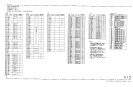
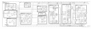
Frequency
Span
Register
(ij
and
Span
Width
DAC
@
The Span Width DACs U17 and
UlO
provide a negative scan ramp to be scaled by the
Integer Number Attenuator. The output of this negative-going ramp is between 0 and -10
V. The amplitude of the ramp is dependent on the span of the instrument. Frequency span
information arrives on the Instrument Bus and is stored in registers
Ul
and U18. This
information is clocked into Frequency Span registers U16 and U18 whenever control line LSAS
(Low = Scan Attenuator Strobe) goes low.
Integer Number Attenuator
@,
Band
Decoder
@,
Switch
Drivers
@I
The Integer Number Attenuator scales the negative ramp at TP5 to the harmonic band being
swept. This division is by
l/2
for Band C,
l/3
for Band D, and
l/4
for Band E. In Band B,
the ramp is not scaled so it remains unchanged.
The division is performed by R48 through R50. If in Band B, only R80 is in the circuit. In
Band C, R81 is added. In Band D, R82 is added. In Band E, R83 is added. These resistors
are switched in by transistors Q15, Q13, and Q14, which are driven by drivers U19A, U19C,
and UlOB respectively. The information necessary to determine when and which resistors to
switch in comes form the Al2 Front-Panel Interface (SAT 1 and SAT 2) and is decided by
Band Decoder P.
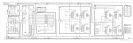
Aux
Out
Register
0,
Aux
Out
Offset
DAC
0,
and
Aux
Out
Amplifier
@I
The AUX OUT signal is a positive-going ramp voltage from the scan generator which is
amplified by U9B. This output is always 0 to
+lO
V regardless of the selected frequency span.
If more than one harmonic band is swept, there is a small ramp output from the ramp
generator E (TP3) f
or each band with each ramp resetting to 0 V. To combine these ramps,
Aux Out Offset DAC U22 and U9A provide a voltage to hold the Aux Out Amplifier input at
a dc level at the end of each ramp. The output therefore is a continuous ramp voltage from
0 to
+lO
V. This voltage is programmed into the DAC U22 by the span information from
the Instrument Bus. This information is stored in Aux Out Register U23 and U21, being
clocked in by control line LAOS (Low = Aux Out Strobe). This control line is from the Al2
2 Al6