


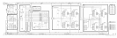
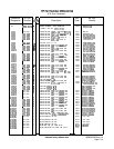

Al6
Al6
Scan
Generator,
Circuit
Description
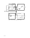
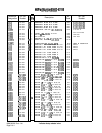
The Al6 Scan Generator provides tuning voltage ramps to the IF-Display Section (SCAN
OUT and AUX OUT)
an
d
scaled ramps to the AlOA8 PLL2 Discriminator and A19 DAC.
The SCAN OUT ramp to the IF-Display Section is used for the horizontal sweep signal for
the CRT display update, and the AUX OUT ramp is used by the
A4Al
Video Processor to
maintain video information in proper correlation with the horizontal sweep and frequency
tuning.
The scaled ramp to the AlOA8 PLL2 Discriminator is used to scale the tuning current ramp
(VCO TUNE)
used to tune the VCO on the AlOA5 PLL2 VCO.
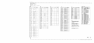
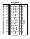
Scan
Time Register
@
and
Sweep
Time
DAC
@
Scan time information is placed in the scan time registers U26, U27, and U29. This
information comes from the front panel via the Instrument Bus. Processing of this
information is done on the Al2 Front-Panel Interface and Al5 Controller. The information is
clocked into the Scan Time Register by control signal LSTS (Low = Scan Time Strobe). This
control signal becomes active (low) whenever the selected scan time is changed. A positive dc
voltage is developed by U8 corresponding to the programmed sweep time information applied
to the DAC U28. This voltage is between
+0.7
V and
+7.0
V.
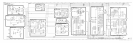
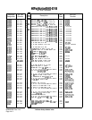
Ramp
Generator
@
The dc voltage level provided by U8 causes a constant current to flow through the proper
scaling resistor, through Virtual Ground and Q5 to the Ramp Capacitor Cl. The scaling
resistor is selected by the programmed sweep information from the front panel the same as is
the sweep time. This information turns on one of the switch drivers U20A through U20D,
which turns on one and only one of the scaling resistor switches
Ql,
Q2, Q3, or Q4, to place
the proper scaling resistors in the charging current path for Cl. If the selected sweep time
is slower than 200 seconds, none of the scaling resistors are switched in. For 0.0 to 2.5 GHz
frequency span, the waveform on Ramp Capacitor Cl is a positive going ramp from -5.0 Vdc
to -2.0 Vdc with a 3 ms reset time. Ramp Buffer U3 amplifies and shifts the level of the
ramp so that the SCAN OUT is a 0.0 to
+lO.O
V dc ramp.
Al6 1