


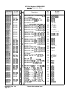
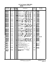
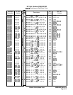

becomes a voltage follower maintaining the voltage at the cathode of CR5 at the same voltage
as on U7 pin 12. In this situation, R32 and R31 are effectively in parallel with the current
sense resistor of the coil driver circuit. R31 is used to adjust the magnitude of compensation,
while R40 is used to adjust the frequency at which the compensation occurs. In a similar
manner, U7A, B, C are used to correct for higher frequency nonlinearity.
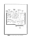
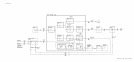
PIN Switch Driver
@
The PIN switch driver converts the TTL logic level LO-BAND signal to the $20
V/-10
V
signal required by the Second Converter. The TTL level at
Pl
to 34 is input to the base of
Q21.
A high at the base of Q21 turns Q21 on, turning on Q4, which pulls the collector of Q4
approximately
+20
V. This turns on Q3, providing the
+20
V signal to the PIN drive output,
Pl
to 35. A low input on the LO-BAND TTL input turns Q21 off, which turns Q4 off. The
collector of Q4 then goes low, turning on Q2, and pulling the PIN drive line to -10 V.
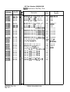
3.3
GHz
Oscillator Driver
@I
The PIN drive signal is also used to turn the 3.3 GHz oscillator on in A-Band, and off in other
bands. When the PIN drive goes high,
Ql
is turned on which pulls its collector to -10 V. The
-10 V is the negative bias for the 3.3 GHz oscillator. When the PIN drive goes low,
Ql
is
turned off, dropping the oscillator bias current to zero, which turns off the 3.3 GHz oscillator.
In the on state, resistor
Rl
is used to adjust the oscillator bias current to 15 milliamps.
RF Switch Driver
@
The coaxial RF switch is driven by darlington amplifiers U5E, and U5F. A high input on the
LO-BAND line drives the outputs of U5F low, and U5E high. A low output at U5F drives the
Coaxial RF switch relay to the A-Band (0 to 2.5 GHz) position. The reverse occurs with a
low input which drives U5E’s output low, which forces the coaxial RF switch relay to the B-E
Band (2 to 22 GHz) position.
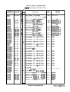
Band Step Gains
@
To correct for different input mixer conversion efficiencies and gains in the individual
frequency bands, the IF gain is changed. This is done in the A6A3 Last Converter by varying
the current through PIN attenuator diodes in the 21.4 MHz amplifier. This current is
controlled by Q12, Q14 to Q17, and
Q19.
In A-Band, the high output on the PIN drive line
breaks down zener
VRl
and turns on
Ql2.
This applies -40 V to the potentiometer R21.
Adjusting R21 varies the current in the step gain in A-Band.
The gain of A6A3 Last Converter is adjusted in each band as each transistor,
Ql2,
Q14 to
Q17, and Q19, is turned on for each individual band.
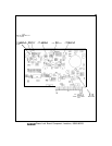
2
A6AlO