


A19
A19
Digital-to-Analog
Converter
(DAC),
Circuit
Description
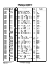
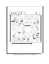
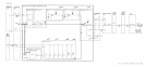
The A19 DAC provides the tuning voltage to the A20 YTO Main Coil Driver used to coarse
tune the YTO Start Frequency and set the proper amount of sweep. This occurs at the
beginning of each sweep and at the beginning of each harmonic band within a sweep.
YTO
Pretune Register
@
and
Pretune
DAC
@
Frequency information is loaded into pretune registers U5 and U6 from the Instrument Bus.
This is coded information from the Instrument Bus. This information is clocked into the
registers by LDAS
(Low
=
DAC Strobe). The Pretune DAC, in conjunction with U2, provides
an output of 0.0 to
i-12.6
V dc in approximately 3
mV
increments. The exact voltage is
dependent on the coded information input. This voltage is applied to Summing Amplifier U4
through R3.
Frequency
Span
Register
and
Switch
Driver
@I
and
Span
Scaling
@
Coded span information from the Al2 Front-Panel Interface is loaded into register U7 from
the Instrument Bus and clocked out to switch drivers U8 and
U9
by LSAS (Low = Scan
Attenuator Strobe). These switch drivers turn on (close) switches
Q2
through Q6 according to
the coded information input. The SCAN DAC IN signal (attenuated sweep ramp) from the
Al6 Scan Generator is then applied to the proper scaling resistors R26 through R30, R38, and
R58, to provide the sweep for the YTO. This output current is applied to Summing Amplifier
u4.
Summing
Amplifier
@
The fixed dc current from the Pretune DAC, corresponding to the desired YTO Start
Frequency, and the ramp current from the Scaling Resistors, corresponding to the desired
Frequency Span, are summed at the input of U4. U4 amplifies this combined signal and
applies it to both the YTO and YTX at a sensitivity of -3
V/GHz
to coarse tune the
analyzer to the selected Start Frequency and Frequency Span.
Negative
Voltage
Reference
@
and
Positive
Voltage
Reference
@
U3 and associated circuitry
0
provide a nominal -12.6 V reference for U3, the pretune DAC
in function block
0.
UlO
and associated circuitry
$J
provide a nominal
+lO
V reference for
summing amplifier U4 in function block
0.
A19 1