


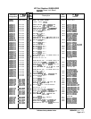
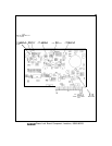
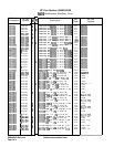

A6AlO
A6AlO
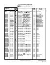
Miscellaneous Bias/Relay Driver, Circuit Description
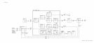
This assembly is a collection of circuits necessary for proper operation of other assemblies in
the A6 RF Module. It contains nine circuits:
1. YTX Diode Bias
2. YTX Linearity Correction
3.
3.3 GHz Oscillator
Driver
4. PIN Switch Driver
5. Band Step Gains
6. RF Switch Driver
7. RF Attenuator Driver
8. j-22 V Delay
9.
Power Down
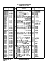
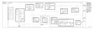
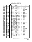
YTX Diode Bias
@
To maintain the precise diode bias across the YTX mixer diode, the effects of series resistance
between the bias circuit and the diode must be eliminated. To do this, a negative impedance
voltage source U2 is used.
Voltage bias to the YTX diode is adjusted from band to band via R9, R12, R15, and R18.
This voltage is applied to U2 via FET switches
QS,
Q7,
QS,
and
&lo.
U2 has both positive
and negative feedback. The positive feedback is controlled by R43, R46, and R47, while the
negative feedback is via R45. The fact that the positive feedback and the negative feedback
are picked off across R44 causes a negative impedance at pin Pl-7 proportional to the
amplifier gain and R44.
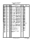
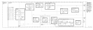
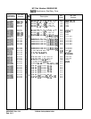
YTX Linearity Correction
@I
Due to nonlinearities in the YTX magnet structure, some linearity correction must be made.
This is accomplished by placing resistors in parallel with the current-sense resistor in the
YTX coil driver circuit. These parallel resistors increase the coil current slightly. For current
compensation, both the point of compensation and the magnitude of compensation must be
varied.
This is accomplished in the following manner using U7D as a typical circuit: U7D is an ideal
zener circuit, that is, as long as the YTX linearity voltage is less negative than the voltage on
U7 pin 12 (the positive op amp input) diode CR5 is reverse biased. In this state, the YTX
linearity line sees a high impedance and no compensation occurs. When the YTX linearity
voltage goes more negative than the bias on U7 pin 12, diode CR5 is forward biased and U7D
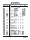
A6AlO
1