


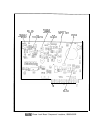
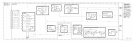
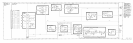

RF Attenuator Driver
@
The RF attenuator driver is similar to the RF Switch driver. The major difference is the logic
decoding to the inputs of the darlington switch drivers. The input to the logic circuit is the
standard 10, 20, 40, dB attenuation logic levels. The logic circuit
Ul
decodes this to the 10,
20, 20, 20, dB attenuation logic levels required to drive the RF attenuator. The output drivers
consist of darlington amplifiers driven by the outputs of
Ul
or the inverted outputs of
Ul,
via
U3. A low output of a darlington turns that line on. That is, a low at U5D pin 13, coupled
with high at U4F pin 11, enables the 10 dB attenuation position, and so forth.
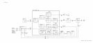
Power Down
@
The power down circuit switches the RF attenuator into a 40 dB attenuation position to
prevent accidental damage to A6A8 YTX or A6A6 First Converter from an input signal when
the instrument is off. When the power up signal goes low, U3 pin 10 is driven high which
turns on
Q9
and Q13, forcing
Ul
pins 5,6, and 9, U4 pin 7, and U3 pin 5 high. This forces at
least the last two 20 dB attenuation stages in the attenuator on.
+22 V Delay
@I
On power up, the instrument goes through a self-check program. To prevent the RF relays
and the attenuator from chattering during this time, the
+22
V Bias to the attenuator and
RF switch is delayed for about 2.5 seconds after the power up signal goes high. This delay is
caused by R59 and ClO. When power up goes high, it takes approximately 2.5 seconds for the
voltage across
Cl0
to charge up enough to turn on U3E. U3E output is inverted twice by the
darlington amplifiers U4B and U4A so that when U3E output drops, U4A output also drops
turning on
Qll
which applies the
+22
V to the relay circuits.