


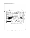

This information is decoded by U3A and amplified by U5. The outputs of U5 are
approximatley
+3
V when a band is valid and approximatley -22 V otherwise. These signals
are used to drive FET switches on the
A6All
Slope Generator and the A6A12 YTX Driver.
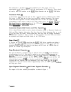
Preselector Peak
@J
A second latch, UlO, receives the same six lines a U9, but receives a different strobe, LCK5.
This strobe is valid when the six lines have preselector peaking information. The outputs
of this latch drive eight bits of a DAC which produces 0 to 10 V at the output of
U4B
corresponding to DAC values of 0.00 to 63.75. This voltage goes to the A6A12 YTX Driver.
This circuit is used to adjust the tacking of the YTX when [PRESELECTOR PEAK) or
(SHIFT)
a),
(K)
(+dBm),
or
(SHIFT)
Ide]
is keyed in.
Hysteresis, Sample-Hold Control, and Filter Capacitor
@
U8 is a Quad D-Latch which is used to decode information relating to Hysteresis, Sample and
Hold, and Filter Capacitor information. Four lines from the 50-wire Instrument Bus go to the
inuts
of the latch. The latch is strobed when these lines have valid RF Module information.
The instrument controller is able to connect the filter capacitor across the YTX, and control
the Hysteresis and Sample and Hold circuits on the YTX Driver.
Slope Offset
@
U7 receives the -0.525
V/GHz
signal from the A6A12 YTX Driver, amplifies and offsets it
such that a
t1.83
V/GH
z ramp centered about 6 V is produced at TP8.
Qll
to Q15 and
associated circuitry produce the offset for each band, and R2 varies the A-Band offset to
position the A-Band slope breakpoints.
Slope Breakpoint Generator
@
The signal at TP8 has a maximum range on Band C (5.8 to 12.5 GHz, second harmonic)
of approximately 0 to 12 V. This signal is applied to two voltage dividers
R36/R37
and
R38/R39,
which
drive the positive inputs to U6A and
U6B
respectively. The voltage at the
inputs to these op amps is clamped by CR5 and CR6 such that U6A sees only the first half
of the full band ramp and
U6B
sees only the second half. In this manner, each full band
is divided into two segments with one breakpoint in the center. Both U6A and
U6B
are
configured for a gain of 2 and an offset of approximately -6.2 V, for a 0 V output at
midband
and unity gain overall.
Upper Segment Generator
@
and Lower Segment Generator
@
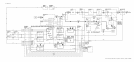
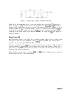
The outputs of U6 drive variable gain amplifiers as shown in Figure 1.
2
A6All