


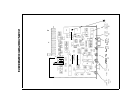

Analog
Integrator-Sample
and
Hold
@
U2 and C7 form an integrator which integrates current flowing from U3 through R8. The
output of the integrator is summed with other signals in U4 and ultimately controls the VCO
frequency. In steady state conditions, TP3 will settle to a constant voltage which tunes the
VCO to the correct frequency. If the voltage at TP3 is constant, the input current must be
zero, so opening FET switch Q3 will not change the voltage at TP3. When PLL2 is being
used in its swept mode, the loop is locked to a start frequency set by AlOA7 PLL2 Divider,
then Q3 is opened. This breaks the lock loop, permitting a sweep to be executed.
Q3 is closed with zero gate voltage, and open with -7 V gate voltage. The gate drive comes
from Q6 and Q7, which translate the TTL level lock-sweep signal on Pl-2 to the
O/-7
V
levels. Pl-2 is also connected to U6A and
QS,
which results in zero voltage at
TPl
during a
sweep. A negative voltage may turn on Q3, changing the charge stored on C7.
Digital
Integrator
@
The analog integrator does not have sufficient control range to correct initial warm-up drift
and long term aging. If TP3 goes below -4.7 V, Q5 is turned on and its collector voltage is
pulled down to -1.4 V. At this point, CR4 and CR3 become forward biased, clamping U2
and
preventing further negative movement of TP3.
Simultaneously, the input of
U7B
will have been pulled low, which turns on a 2 kHz oscillator
made up of U7C, R20, and
Cll.
This clocks the count up input of counters U8 and U9,
which drives DAC UlO. UlO sources negative current to the summing junction of U4 and this
current increases in magnitude as U8 and
U9
count up. When the current reaches a value
which tunes the VCO to the proper frequency, TP3 moves positive, shutting off the oscillator
and returning control to the analog integrator. An analogous sequence occurs when TP3 tries
to rise above
+5.7
V.
Output
Amplifier
@
U4 serves to sum signals from the analog integrator, DAC, and
Rll.
Rll
is a high frequency
signal path shunting the integrators.
2
AlOA6