


E6581301
H-11
8
8.4.2 Monitor display at tripping
At the occurrence of a trip, the same information as that displayed in the mode described in 8.2.1, “Status monitor
under normal conditions,” can be displayed, as shown in the table below, if the inverter is not turned off or reset.
To display trip information after turning off or resetting the inverter, follow the steps described in 8.2.2, “Display of
detailed information a past trip.”
■
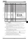
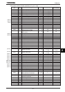
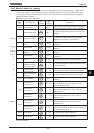
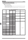
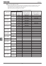
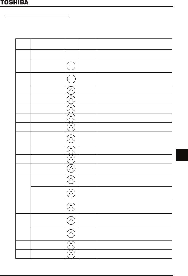
Example of call-up of trip information
Commun
ication
No.
Item displayed
Key
operated
LED
display
Description
FC90 Trip information R
Status monitor mode (The code blinks if a trip occurs.)
The motor coasts and comes to a stop (coast stop).
- Setting monitor mode
CWJ
The first basic parameter “History function (CWJ)” is
displayed.
FE01 Direction of rotation
HTH
The direction of rotation when the trip occurred is
displayed.(H:Forward run, T:Reverse run)
-
Frequency command
value
The operation command value when the trip occurred
is displayed.
- Output current E
The inverter output current at tripping (load current) is
displayed.
-
Input voltage (DC
detection)
[
The inverter DC voltage at the occurrence of a trip is
displayed.
- Output voltage R
The inverter output voltage at the occurrence of a trip
is displayed.
- Torque S
The torque when the trip occurred is displayed.
-
Regenerative braking
resistance overload
factor (PbrOL data)
T
The regenerative braking resistance overload factor at
tripping is displayed.
-
Inverter overload
factor (OL1 data)
I
The inverter overload factor at tripping is displayed.
-
Motor overload factor
(OL2 data)
N
The motor overload factor at tripping is displayed.
FE00 Output frequency
The output frequency when the trip occurred is
displayed.
FE06
Input terminal
information 1
The ON/OFF status of each of the control input
terminals at tripping (F, R, ST, RES, S1, S2, S3,
RR/S4) is displayed in bits.
Input terminal
information 2
C
The ON/OFF status of each of the optional control
input terminals at tripping (LI1, LI2, LI3, LI4) is
displayed in bits.
Input terminal
information 3
D
The ON/OFF status of each of the optional control
input terminals at tripping (LI5, LI6, LI7, LI8) is
displayed in bits.
FE07
Output terminal
information 1
The ON/OFF status of each of the control output
terminals at tripping (OUT1, OUT2 and FL) is
displayed in bits.
Output terminal
information 2
The ON/OFF status of each of the optional control
output terminals (OUT3, OUT4, R1, OUT5, OUT6, R2,
R3, R4) is displayed in bits.
FE08 CPU1 version X
The version of the CPU1 is displayed.
FE73 CPU2 version Y
The version of the CPU2 is displayed.
(Continued overleaf)
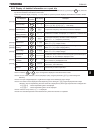
*1
MODE
[Note 4]
*2
*5
*6
*7
[Note 4]
[Note 5]
*3
[Note 4]
*4
*8
[Note 6]
[Note 3]
MODE