


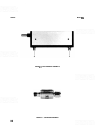


MODEL
8559A
SERVICE
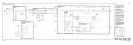
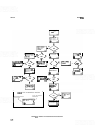
FREQUENCY CONTROL ASSEMBLY A7, CIRCUIT DESCRIPTION
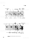
The Frequency Control Assembly A7 drives the YIG-Tuned Oscillator Assembly A6 and provides the regulated
+
14.5V and
-
10V supplies to the First Mixer Assembly A4, the Second Converter Assembly AS, and the
Marker Assembly
A8. Inputs to the Frequency Control Assembly A7 consist of the tuning voltage and the band
information from the Front Switch Assembly
A2,
as well as the attenuated sweep from the Marker Assembly
A8. The tuning voltage is routed to the Marker Assembly A8 while the sweep plus tune (S
+
T) voltage goes to
the Step Gain Assembly A12 and Vertical
Driver/Blanking Assembly A15. The YIG Tune Voltage (YTV) is
applied to the biasing circuitry of the YIG
-
Tuned Oscillator Assembly A6.
TunelFull Span Voltage (B)
Coarse and fine tune voltages from the front panel are summed and buffered by U12 and resistors R77, R78,
and
R79. This summed voltage is routed to the YTO Main Coil Tune Driver through Q13.
It
is also routed to the
Marker Assembly A8 to be conditioned for the Digital Panel Meter Assembly
A1
.
Resistors R64 and R65 divide
the
-
10V supply to develop
-
5V at the noninverting input of U11, which buffers the voltage for use as the
mid-band tune voltage required for full sweep operation.
With the selection of full sweep operation,
PI-41 (FS9) goes to
+
15V and Qll turns off. Without current
flowing in R90,
Q10 is off. This allows Q9 to turn on because Q10 no longer supplies the positive gate
-
source
voltage that holds Q9 off. At the same time,
412 turns on, shutting 413 off. This routes the
-
5V supplied by
U11 to the YTO Main Coil Tune Driver tuning the YTO to mid
-
band. When full band is not selected, PI-41
(FS9) is close to ground potential due to A8CR19, A8R91, and A8R92, on the Marker Assembly A8 (block B).
This results in
Q10 turning on, holding Q9 off. Transistor A12 is now turned off, removing the pinch
-
off
voltage on
413. The tune voltage from the front panel now adjusts the YTO center frequency.
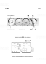
YTO Main Coil Tune Driver
(D)
Operational amplifier U10 and resistors R61, R62,
R72,
R76, R80, and R82 sum and offset the applied tuning
and sweep voltages and convert them to the current required to tune the YTO. The current is set by the voltage
across R48 and the 6
GHz adjustment R47. Shaping of the voltage-to-current function is necessary to maintain
the linearity of the YTO sweep. This shaping is accomplished by using CRS, in conjunction with
R59* and
R60*, to establish two break points in the sweep ramp. MOSFET Q8 adds current drive capacity to the output
of
U10. Offset and buffering of the sweep plus tune voltage takes place in U9. It supplies the sweep plus tune
voltage to the limit comparator on the Vertical
Driver/Blanking Assembly A15 and to the first converter band
tilt circuit on the Step Gain Assembly A12. Operational amplifier U9b supplies the YIG Tune Voltage (YTV) at
1V per GHz to the biasing circuitry of the YTO. This adjusts the YTO, controlling its harmonic output. Delay
compensation for main coil sweeps is provided by C 12* and
R58.
FMlMain Coil Sweep Switch (A)
Quad switch U15 routes the attenuated sweep ramp to the YTO Main Coil Tune Driver or to the YTO FM Coil
Driver while grounding the unused inputs. Transistor
416 provides level shift for the switch drive and is con-
trolled by the FREQ
SPAN/DIV control.
YTO FM Coil Driver
(G)
The YTO
FM
Coil Driver sweeps the YTO in spanwidths of 1 MHz per division and narrower. Operational
amplifier U13 inverts the sweep voltage and drives the push
-
pull current driver comprising 414 and Q15.