


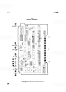

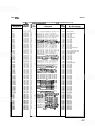
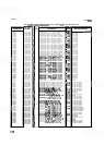
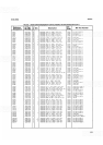

SERVICE
MODEL
8559A
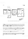
switch that connects R34 to the comparator. Turning the manual sweep control
(A2R4)
adjusts the voltage at the
control side of R34.
Operational amplifier U 1, operating in a linear mode, fixes the voltage at pin 2 by feedback through
CR2, the
buffer amplifier, and
R29. This fixed voltage is applied through 439 to one side of R34. As the manual sweep
potentiometer is adjusted, the voltage across R34 changes, varying the current supplied to pin 2 of the compara-
tor. This current is forced through R29 and develops the voltage offset that varies the ramp voltage.
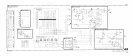
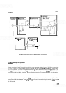
Current Source
(F)
The current source provides a constant charging current to the timing capacitors (block I) at a rate selected by
either the SWEEP
TIME/DIV switch or the automatic sweep time (AST) line.
Temperature compensation of the current source is accomplished by the nominal
+
10V supplied by the temper
-
ature
-
dependent power supply (block P). The 1 MS (one millisecond) adjustment fixes a voltage at pin 3 of U2a,
while the 5 MS adjustment varies the feedback around U2a.
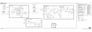
During calibrated sweep time settings, the Sweep Cal. Switch (Qll in block G) is off. This allows the feedback
ratio of
U2a, the voltage source, to be varied by grounding different input resistor combinations (R21 through
R24) with the SWEEP
TIME/DIV switch. In the automatic sweep mode, Sweep Cal. Switch Qll is turned on
by current through Q9 and R25. The feedback ratio now varies with the resistors attached to the AST line and
switched in by various settings of the FREQ
SPAN/DIV and RESOLUTION BW switches. When the video
filter is on, it also affects the feedback and, therefore, the sweep time, by varying the voltage at the emitter of
Q8a.
The voltage applied to the emitter of Q8a from voltage source U2a is proportional to the logarithm of the sweep
time. Transistor Q8a converts this voltage to a current directly proportional to the sweep time, which charges
the timing capacitors in the buffer amplifier. A current limiter composed of
Q5 and R15 limits the automatic
sweep time to about 1.5 milliseconds per division.
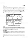
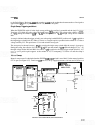
Xtal Resolution Bandwidth Control (B)
When the RESOLUTION BW switch selects a crystal filtered bandwidth (530 kHz), bandwidth control line
BW5 is open and pulled to
-
0.5V by 412 and Q10 in the Xtal PIN Driver Buffer (block
D).
As a result, four
simultaneous changes occur in the analyzer: the crystal poles on the Bandwidth Filter assemblies are activated,
the LC poles are disabled, the crystal bandwidth-control current is established, and the automatic sweep time is
scaled for the crystal bandwidths.
Control line
BW5, from the RESOLUTION BW switch, is routed to the Bandwidth Filter assemblies (A1 1 and
A13) where it activates the crystal filter poles. (Refer to Bandwidth Filter Assembly No. 1 All, Circuit Descrip-
tion and Schematic.) It reverse biases A1
1/A12CR2 (block D) and A1 1/A13CR13 (block
G).
At the same time,
A1
l/Al3Q3 and A1 1/A13CR8 (block D), and A1 l/Al3Q6 and A1 l/A13CR15 (block G) are turned on.
The LC poles on the Bandwidth Filter assemblies are disabled by a positive voltage on the BW7 control line.
Voltage for BW7 is generated in the LC PIN Driver Buffer (block C) on the Sweep
Generator/Bandwidth
Control Assembly A9. Control line BW5 turns A1 l/A13Q22 off, allowing BW7 to be pulled to a level greater
than
+
1OV by A1 l/A13CR17 and A1 l/Al3RlO5. This turns off the LC filter sections.