


MODEL 8559A
SERVICE
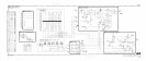
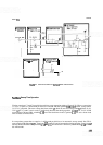
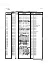
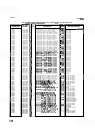
Crystal filter bandwidth is determined by the current on BW6. Transistor 413 in the Xtal PIN Driver Buffer
(block D) is turned off, allowing
414 to establish the bandwidth control current. Depending on the setting of
the RESOLUTION BW switch, one of the bandwidth control lines
(BWl through BW3) is at
+
15V while the
remaining two are open and pulled to a negative voltage. The positive voltage turns on one of the transistor
switches in the Xtal Resolution Bandwidth Control
(442,444, or 446 in block B). The current on BW6 is now
established by one of the factory selected resistors,
R109, R110, or R111, and the setting of R72 (the crystal
bandwidth adjustment, block D). When the 30 kHz bandwidth is selected, no current is drawn through
414 and
the bandwidth-control PIN diodes (A1
1/A13CR4 and All/A13CR12 on the Bandwidth Filter assemblies) are
off.
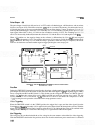
The automatic sweep time (AST) is determined by combinations of resistors switched into the current source
circuit by front panel settings. (See the Current Source circuit description.) These resistors are located in blocks
A, F, 0, and the VIDEO FILTER switch
A2S2. The contribution of the RESOLUTION BW occurs in the LC
Resolution Bandwidth Control (block A). Resistors
R117, R119, R121, and R122 are switched into the AST
circuit by 43 1,
426, 427, and 428, respectively, when the proper control line is activated. Control lines BW2
through BW4 and the noise measure position of the VIDEO FILTER switch apply
+
15V to their respective
control lines. The same lines are used to control sweep times in both crystal and LC modes. Since the same
resistors are used to establish the automatic sweep time for both crystal and LC modes, scaling is necessary. To
scale the sweep time,
424 in block A switches R75 in or out of the AST circuit. During crystal filter operation,
BW5 turns 424 off and removes R75 from the circuit, allowing a longer sweep time.
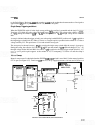
LC Resolution Bandwidth Control
(A)
When an LC filtered bandwidth
(1
100 kHz) is selected, control line BW5 is pulled to
+
15V by the RESOLU
-
TION BW switch. This results in four simultaneous changes in the analyzer: the LC poles on the Bandwidth
Filter No. 1 and No. 2 Assemblies
A1 1 and A13 are activated, the crystal poles are disabled, the LC bandwidth-
control current is established, and the automatic sweep time is scaled for LC bandwidths.
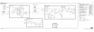
With
+
15V routed to the Bandwidth Filter assemblies by BW5, A1 1/A13Q3, A1 1/A13Q6, A1 1/A13CR8, and
A1
1/A13CR15 are turned off and A1 1/A13CR2 and A1 1/A13CR13 are on. (Refer to Bandwidth'Filter Assem-
bly No. 1
A1 1, Circuit Description and Schematic.) This blocks any signal from passing through the crystal filter
sections. Transistor
413 (on the Sweep Generator/Bandwidth Control Assembly A9, block D) turns on and
control line BW6 is pulled to
-
4V, which further inhibits the crystal filters.
The defeat of the crystal filter poles and the application of bandwidth
-
control current on the BW7 line activates
the LC filter sections. The LC bandwidth is controlled by the current through BW7 to the Bandwidth Filter
assemblies. Transistor 422, in the LC PIN Driver Buffer (block C), is turned on, allowing the current on BW7
to be controlled by 421. The position of the RESOLUTION BW switch, via BW2 through BW4, turns one of
the transistor switches
(426, 427, or 431) in the LC Resolution Bandwidth Control (block
A)
on. The band-
width
-
control current on BW7 is now determined by
a
factory selected resistor, either R116, R118, or R120, and
R85 (LC bandwidth adjustment, block C). If the 100 kHz bandwidth is selected, 422 is turned on, but BW7 is
pulled up to greater than
+
10V through R106. The bandwidth
-
control PIN diodes (A1 1/A13CR3 and A1 l/
A13CRll on the Bandwidth filter assemblies) are reverse biased by BW7.
Automatic sweep time scaling for LC occurs when BW5 turns
424 (block A) on. This switches R75 into the
AST circuit and decreases the sweep time. The effect on the automatic sweep time
is
determined
by
the
parallel
combination of R75 and the resistor (R117, R119, R121, or R122) selected by the active control line.