


MODEL 8559A SERVICE
BANDWIDTH FILTERS No. 1 and No.
2
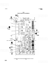
ASSEMBLIES All and A13, CIRCUIT DESCRIPTION
Bandwidth Filters No. 1 and No. 2 Assemblies All and A13 are identical except for some off
-
board connec
-
tions. Bandwidth Filter No. 1 Assembly A1 1 is described here. Bandwidth Filter No. 1 Assembly A1 1 operates
at 21.4 MHz with a variable bandwidth of 3 MHz to 1 kHz. The RESOLUTION BW switch selects one of the
following eight available bandwidths: 3 MHz, 1 MHz, 300 kHz, 100 kHz, 30 kHz, 10 kHz, 3 kHz, or 1 kHz.
Four stages of filtering are used for
all
eight bandwidths; each assembly contains two stages. The bandwidths
from 30 kHz to 1 kHz are obtained from synchronously
-
tuned crystal filters. The remaining four bandwidths
(100 kHz to
3
MHz) use synchronously
-
tuned LC tank circuits. The four crystal filter stages contain factory
selected and matched crystals
(AllYl, A1 1Y2, A13Y1, and A13Y2) that must be replaced as a set. If replace
-
ment of a bandwidth filter assembly is necessary, the new assembly is shipped with two crystals installed and
two packaged separately to replace the crystals on the other assembly. In addition to the filter stages, each board
contains a 10 dB Buffer Amplifier, a Unity Gain Buffer Amplifier, and an Output Buffer Amplifier.
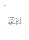
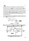
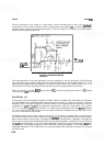
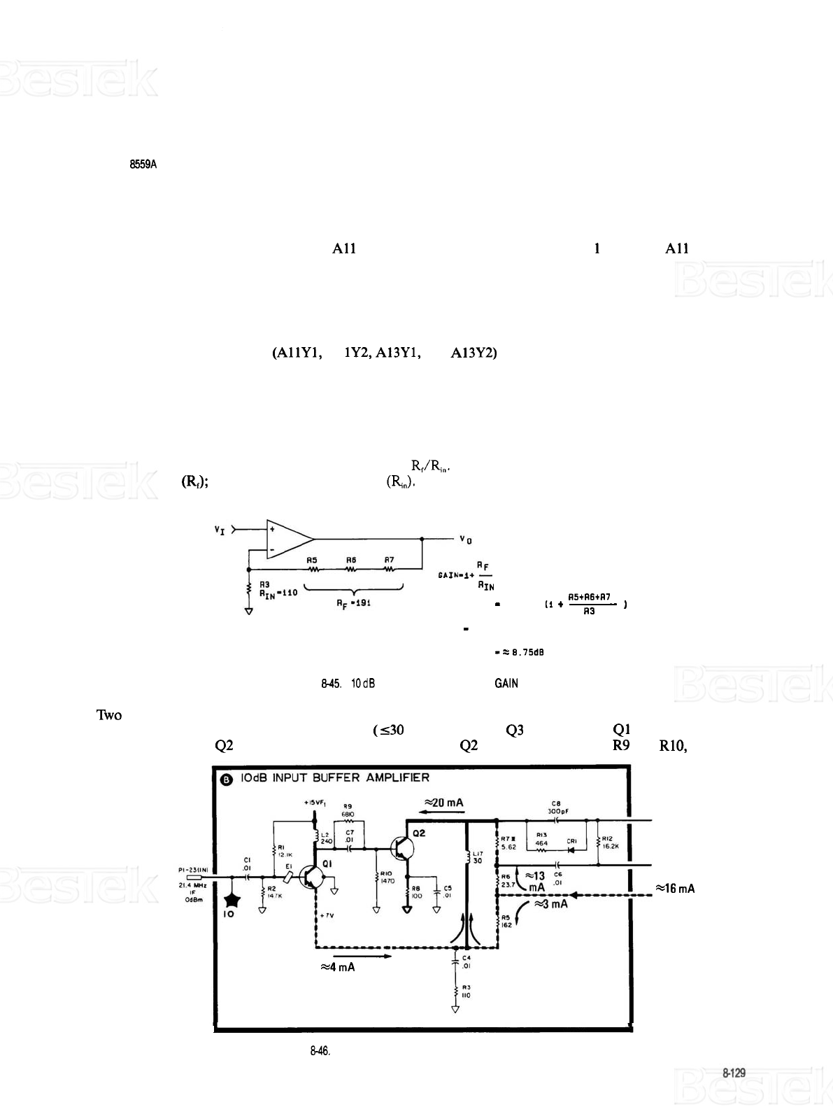
10 dB Input Buffer Amplifier (B)
The 10 dB Input Buffer Amplifier is shown as a noninverting operational amplifier in Figure 8
-
45. Gain for the
amplifier is expressed in the equation: Gain
=
1
+
RJR,,.
The total resistance of R5, R6, and R7 forms the
feedback path
(RJ; R3 forms the input resistance
(R,,).
This ac model of the amplifier's operation is true for all
but the narrowest bandwidths, as illustrated later.
--
-
R1~
R5tR6tR7
GAIN IN dB
-
20
LOG
li
+
-
R3
1
GAIN
-
2.73
GAIN IN dB
-=
8.7548
FIGURE 6-45.
10dB
INPUT BUFFER AMPLIFIER GAIN MODEL
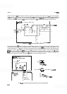
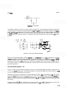
nYo current paths are used for dc bias in the input buffer amplifier, one for crystal filter poles, another for LC
filter poles. When a crystal filtered bandwidth
(530 kHz) is selected, 43 (block
D)
and Q1 are the sources for
the current through
42 (see Figure
8
-
46).
The base voltage of 42 is fixed by the divider R9 and R10, while the
W6
rnA
DC
BlAS
IN BLOCK
D
-
~4
mA
DC
BlAS
FIGURE
846.
DC BlAS PATH DURING CRYSTAL POLE OPERATION