


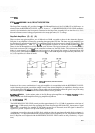

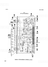

SERVICE
MODEL
8559A
+
5.1
V
Reference
(K)
Transistor
44
and its associated circuitry operate off the
+
15V supply to furnish a regulated
+
5.1V reference
for the flatness and mixer diode bias circuit.
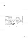
Power Supplies
(J)
Extensive filtering of the
+
15V,
+
12V, and
-
12.6V inputs is needed to reduce coupling between each step gain
amplifier and between the Step Gain Assembly A12 and the other assemblies.
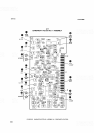
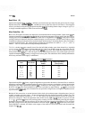
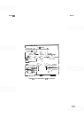
STEP GAIN AMPLIFIER ASSEMBLY A12, TROUBLESHOOTING
Tubular ceramic capacitors will short to the aluminum extrusion if allowed
to touch it during testing.
Always check the supply voltages. If the
+
15V supply drops (even slightly), the
+
5.1V Reference becomes
unregulated.
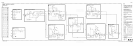
Linear or Log Fidelity Errors:
First readjust REFERENCE LEVEL FINE to the
-
12 dBm position and
test again. If the problem is not present, gain compression may be occurring in one of the circuit's amplifiers.
The 10 dB Amplifier (block
E)
is the most probable source, and improper biasing of CRl is the most probable
cause. Insufficient dc biasing of
CR1 allows signal voltage to vary the bias, causing the stage gain to vary as the
signal level varies. Diode
CRl, not transistor saturation, is the most common cause of compression.
Reduction of the losses in the
0
-
12
dB
Control (block
H)
allows the first amplifier stage to operate at a lower
input level, thus reducing compression. To decrease the losses, hand-select CR7 and C23 for minimum circuit
loss.
Poor Linearity of the
0
-
12 dB Control:
The most probable cause is CR7.