


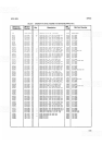
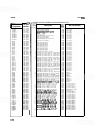


MODEL
8559A
SERVICE
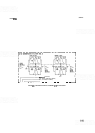
LOG AMPLIFIER ASSEMBLY A14, CIRCUIT DESCRIPTION
The Log Amplifier Assembly A14 includes seven amplifier stages, each capable of providing linear and loga-
rithmic amplification. A detector circuit following the amplifier stages
detect.7 the amplified 21.4
MHz
IF
signal, producing the vertical display signal. The offset circuit that follows the detector operates in Log mode to
offset the vertical display signal in 100 mV steps. This steps the display in four 10
-
dB increments of apparent
gain and adds the last 40 dB of displayed step gain to the gain
(50
dB) already provided in the IF section.
AmplifierStages(Istthrough7th)
(A) (C) (D) (E)
(F)
(G)
(H)
The seven amplifier stages are similar in operation. Different stages are selected as linear or log amplifiers,
depending on the setting of the Amplitude Scale switch.
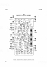
Log Mode of Operation.
In Log mode, the gain of the seven amplifier stages is sequentially limited as the
signal level increases. Limiting starts with stage seven, since it sees the combined gains of the other stages, and
continues sequentially as the signal level increases. Stage one is the last stage to begin limiting the signal. The
total limiting process provides 70 dB of log display range. Each stage consists of an emitter follower
voltage-
driver and a common-base amplifier in which the gain is signal-level dependent. Increases in signal level
decrease the gain.
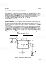
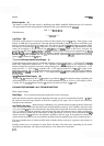
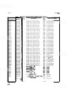
A simplified schematic of a typical log stage (the second stage) is shown in Figure
8
-
64.
In Log mode, the LOG/
LIN control line is high (about
+
15V); 424 is on, forward biasing diodes CRlO and CRll and the log diodes in
all of the other stages. Diodes CRlO and CRll are Schottky diodes with a forward bias voltage of approxi-
mately
0.4V Emitter follower 413 is a voltage source that develops signal current flow through CRlO and
CRl 1
.
This signal-current drives 420, a common
-
base amplifier tuned to approximately 21.4
MHz.
The gain of
this amplifier is set by the ratio of R52 to the total resistance, R,, between the emitters of
413 and 420
(primarily the resistance of CRlO and
CR1 I). The formula for computing the gain in dB is:
Gain (dB)
=
20LOG(1
+
R52/RT)
/
SECOND
STAGE
\
SIGNAL PATH
4
CA1l
C6
.Ol
Y
I
+15V
LOG/LIN
CONTROL LINE
FIGURE
8
-
64.
LOG MODE OPERATION, SIMPLIFIED SCHEMATIC