


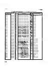


SERVICE
MODEL 8559A
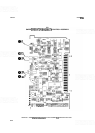
IF Preamplifier
(F)
The IF Preamplifier voltage gain is provided by Q8 in a common
-
emitter amplifier configuration. Circuit gain is
controlled with collector
-
to
-
base feedback through PIN diode CR4. The current through CR4 is adjusted from
the front panel by the
REF
LEVEL CAL control and can vary the gain of the IF Preamplifier over a 10 dB
range. Transistor
47 functions as an emitter follower buffer amplifier.
Flatness Compensation Amplifier
(H)
Approximately 20 dB of compensation is available in the Flatness Compensating Amplifier to compensate for
small changes in conversion efficiency that occur while sweeping through individual bands. Larger
between-
band changes in conversion efficiency are compensated for in the Band Conversion Loss Amplifier. The gain of
the Flatness Compensation Amplifier is controlled by the Non
-
Linear Current Source, which draws current
through PIN diode
CR1. The more current it draws, the lower the gain.
Non-Linear Current Source
(G)
The flatness voltage from the Step Gain Assembly A12 sets the base voltage of 43. Resistors R41, R42, R43,
and diode
CR5 establish the emitter current and cause it to vary non
-
linearly in response to changes in the base
voltage. This non
-
linear current drives CRl and enables the gain of the Flatness Compensation Amplifier to be
proportional to the base voltage (and flatness voltage) at about
0.4V per dB of gain.
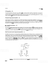
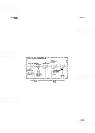
Band Conversion Loss Compensating Amplifier (I)
The Band Conversion Loss Compensating Amplifier changes gain in discrete steps to compensate for the
changes in conversion Ioss associated with RF section harmonic band switching. In the fundamental mixing
bands (Bands 1 and 2), the circuit has unity gain. During second harmonic mixing (Bands 3 and 4),
CR2 is
forward biased, allowing the gain to be set by R34 as shown in the following equation:
Gain
=
1
+
R32/R34.
In the third harmonic mixing mode (Bands 5 and 6), CR3 is forward biased and R36 establishes the gain as
follows: Gain
=
1
+
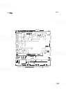
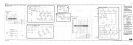
R32/R36. See Figure 8
-
41 for a simplified schematic of the Band Conversion Loss
Compensating Amplifier gain switching. A gain
-
versus
-
band table is shown on the Third Converter Assembly
A10 schematic below function block I.
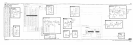
FIGUREMI. BAND CONVERSION LOSS COMPENSATION AMPLIFIED GAIN SWITCHING, SIMPLIFIED DIAGRAM