


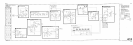
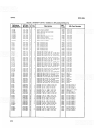


MODEL 8559A SERVICE
When the 1 kHz bandwidth is selected, CR4 is biased on and has a resistance of about
60
ohms. This resistance
forms a voltage divider with
R,
that results in signal amplitude loss across the crystal. Increased gain in the input
buffer amplifier, caused by the load on 43, compensates for these losses. The gain increase occurs when the
reduction in
R,
turns 43 on even harder, resulting in some of the feedback from R6 being shunted to ground
through the collector of 43. This reduction in negative feedback increases the gain of the input buffer amplifier.
By substituting into the gain formula the 1 kHz bandwidth
R,
(10
+
60
=
70 ohms), a new gain of 4.0 (12 dB) is
derived.
First
Xtal
Pole
(D)
Crystal filtering is used for bandwidths of 1 kHz, 3 kHz, 10 kHz, and 30 kHz. Individual poles have a band
-
width about 2.3 times the selected bandwidth, and each filter board assembly (two poles combined) has a
bandwidth of about 1.5 times the selected bandwidth. For example, when the 1 kHz bandwidth is selected, each
pole has a 3 dB bandwidth of about 2.3 kHz, each assembly a bandwidth of 1.5 kHz. The signal from the input
buffer amplifier is routed to 43 and to compensation amplifier 44. (The action of 43 is discussed in the 10 dB
Input Buffer Amplifier description.) From 43 the signal is applied to the crystal
(Yl), where it is filtered before
going to the unity gain buffer amplifier.
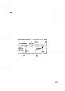
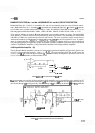
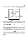
The crystal functions as a series
-
resonant filter tuned to 21.4 MHz.
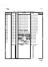
An
equivalent circuit is shown in Figure
8
-
49. Parallel capacitance C, is the result of terminal and case capacitances in the crystal;
R,
is the effective
resistance at resonance (about 10 ohms). Both
C, and R, are detrimental to the pole's performance, so
compensation is used to nullify their effects. Because they are cancelled,
C, and
R,
are not shown in the
simplified crystal pole schematic.
FIGUREJ3
-
49. CRYSTAL MODEL
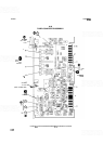
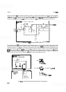
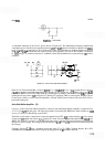
Pin diode CR4 (see Figure 8
-
50) controls the filter's bandwidth by functioning as a variable resistance at 21.4
MHz. The voltage applied to
BW6F controls the current through CR4 and its resistance.
An
increase in current
decreases the resistance and narrows the bandpass.
The crystal presents a low impedance
(R,)
to the signal at resonance, hence signal voltage is developed across
CR4. As the signal frequency varies from the center frequency (21.4 MHz), the impedance of the crystal
increases, making it part of a voltage divider with CR4 and causing more signal voltage to be developed across
the crystal. The frequencies at which crystal impedance and PIN diode resistance become equal are the
3
dB
points of the bandpass. Varying the PIN diode resistance, therefore, varies the bandwidth.
FIGLJRE
8-50,
FIRST CRYSTAL POLE, SIMPLIFIED SCHEMATIC