


SERVICE
MODEL
8559A
Video
Filter
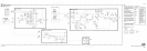
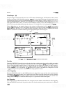
The video filter comprises control A2R6, RESOLUTION BW switch A2AlS5, and eight capacitors on the
Sweep
Generator/Bandwidth Control Assembly A9 (blocks A and B). VIDEO FILTER control A2R6 varies the
resistance of the RC filtering network that it forms with the video filter capacitor. The RESOLUTION BW
setting determines which video filter capacitor
will
be
switched in by the transistor switches (441, 443, Q45,
and
447 in crystal bandwidths, and 454, 432, Q30, and Q55 in LC bandwidths). Increased capacitance is
switched in to provide increased filtering as the bandwidth narrows.
The output of the Xtal PIN Driver Buffer
(BW6) is applied to the bases of 442, 444, 446, and 447 via CR18
through
CR21. This holds the transistors off and prevents the crystal mode, video filter capacitors from being
switched into the circuit during LC mode operation. It is not necessary to switch the LC mode video filter
capacitors out of the circuit during crystal operation; their values are so much smaller that they are effectively
out of the circuit.
Switch
A2S2 applies maximum video filtering for noise measurements by turning on Q55, which switches in
C28.
Sweep
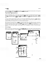
Attenuator (0)
The Sweep Attenuator circuit attenuates the full span sweep
(
-
5V to
+
5V), before it is applied to the Fre
-
quency Control Assembly A7, as a function of the FREQ SPAN/DIV setting. The circuit also varies the
automatic sweep time (AST) as a function of the frequency span. Attenuation takes place in the 1
-
2
-
5
-
10
sequence that results in the FREQ
SPAN/DIV control sequence. The circuit has two voltage dividers separated
by U3, the unity gain sweep buffer. The input divider provides divide
-
by
-
two and divide
-
by
-
five; the output
divider provides divide
-
by
-
ten and divide
-
by
-
one
-
hundred.
To select any of the input dividers,
+
15V is applied to activate the associated control line. For example, if FS3 is
activated, Q51 and
QSO turn on and ground R102 and R73. Resistor R102 becomes part of the AST circuit; R73
forms a divider with R70 that results in the ramp voltage being divided by two. The divided ramp is then applied
to the sweep buffer.
The dividers at the output of the sweep buffer have reversed control
-
logic. That is, they are normally connected
to
+
15V by the FREQ SPAN/DIV switch and open
(OV)
when selected. Transistor Q19 is a gate to drive 417.
When FS4 and FS5 are connected to
+
15V, Q19 is off. As a result, 417 is on and opens a path for the sweep
buffer's output to P1
-
12. No attenuation takes place. If either FS4 or FS5 opens, Q17 shuts off. When FS4
opens,
416 turns on and a divide
-
by
-
ten (R81/R82
+
R83) is provided. When FS5 opens, Q15 turns on and
provides a divide
-
by
-
one
-
hundred (R81
+
R82/R83).
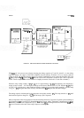
Automatic sweep is varied as a function of frequency span by transistors 453, Q51, 449, 429, 425, and 423.
Transistor
A29
is switched on in narrow spans
(<1
MHz/div) when the YIG FM coil is swept.
All
of these
transistors act as switches connecting resistors from the AST line to ground. This varies the sweep time. (See the
Current Source circuit description.) As the FREQ
SPAN/DIV is narrowed, the sweep time is decreased.
Sweep
Offset
Transistor 420 in the sweep attenuator (block 0) makes it possible to offset the sweep ramp in response to the
position of a start
-
center (ST
-
CTR) switch. This capability is not required in the HP 855949. So, the
+
15V from
the Motherboard Assembly A16 is applied to
420, holding it off. The circuit is always in the center position.
8104