


MODEL 8559A
SERVICE
VERTICAL DRlVlNGlBLANKlNG ASSEMBLY
A15,
CIRCUIT DESCRIPTION
The Vertical Driving/Blanking Assembly A15 contains a preamplifier to amplify the detected and filtered video
received from the Log Amplifier Assembly A14. It also supplies the video signal needed to trigger the sweep
generator in the video trigger mode. Following the preamplifier is the vertical driver, a differential amplifier that
drives the vertical deflection plates in push
-
pull. Blanking, penlift, retrace, and sweep indicator signals are also
supplied by the Vertical
Driving/Blanking Assembly A1 5.
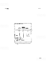
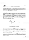
Preamplifier (A)
The detected and filtered video (0 to 800 mV) from the Log Amplifier Assembly A14 is applied to the gate of
Q17a. Transistors 417 (both sections), Qll, 412, and 418 form an FET input differential amplifier; the gate of
Q17a is the noninverting input and the gate of Q17b is the inverting input. The amplifier's output, at the emitter
of
418, is fed back to the inverting input (Q17b) through a voltage divider (R11, R12, and R13). A simplified
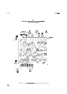
preamplifier circuit diagram is shown in Figure 8
-
70. The voltage gain can be expressed as a function of these
resistor values: Gain
=
1
+
Rl l/R12
+
R13. The circuit's gain is 10. Since the limit to the input voltage is 800
mV, the maximum voltage at the output of 418 (TP3) is
8V.
This voltage is coupled through R17 and becomes
the trigger voltage for the video trigger mode (VIDEO position). Transistor array section U2d and transistor
413 are temperature
-
compensated current sources. These bias the differential amplifier (U2a, U2b, and Q20)
that provides isolation between the preamplifier and the vertical driver. The preamplifier output is sent via
R40
to the rear panel (AUX
VERT
OUTPUT, P 1 pin 14).
FIGURE
8-70, PREAMPLIFIER CIRCUIT, SIMPLIFIED SCHEMATIC
Since the vertical driver deflection sensitivity is 800
mV,
for full
-
scale deflection, a divide
-
by
-
ten circuit and an
offset circuit are used to obtain the correct signal amplitude. With the
LOG/LIN switch (A2AlA2) in either the
10 dB per division or linear position,
+
15V is applied to the EXPAND line. This reverse biases CRl and turns
Q19 on, dividing the preamplifier's output by 10. Diode CR2 is forward biased and diode CR3 is reverse biased.
Transistor Q19, R18, and R20 form the output divider network. When 1 dB per division is selected, the
EXPAND line is open and Q19 is biased off by
CR1 and R22, disabling the divide
-
by
-
ten circuit. The full
preamplifier voltage is now available at the output of
418 and must be offset
+
7.2V to display the 800 mV
signal peak. This in effect expands the display.
The offset of the signal is accomplished by a circuit comprised of
U2c, CR3, CR4, and R18. Transistor array
section
U2c forms an adjustable current source that draws current through CR3 and R18. The 1 dB offset
control is used to set the voltage drop across R18 at
+
7.2V This voltage shifts the signal negatively
as
it passes
through
R18. Diode CR4, becomes forward biased as the offset signal goes below
-
0.6V
and acts to clamp the
minimum output at that level.