


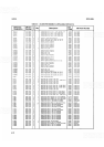
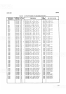

SERVICE
MODEL
8559A
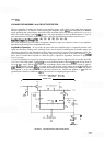
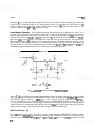
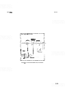
Buffer Amplifier (L)
The detector's output, the video signal, is amplified by the Buffer Amplifier. Differential pair 421 and driver
422 approximate a noninverting operational amplifier with a gain calculated by the
formda:
Which becomes:
Gain
=
1
+
RllO/R116
1
+
619/619
=
2
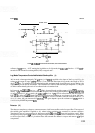
Log Offset
(M)
The offset circuit operates in Log mode to offset the video signal in four 100 mV steps. These appear on the
display as 10 dB steps of apparent gain. This gain adds the last
40
dB of display step gain to the 50 dB of gain
already provided by the Step Gain Assembly A12. The offset is provided by
423 operating as a current source
that steps the current through
R119. When the Log mode is selected,
+
15V via the REFERENCE LEVEL
switch can be applied to IF gain control lines
IFG4,
IFG5,
and IFG6. When an IFG line is activated, the
associated log
-
shift diode (CR31, CR32, or CR33) is forward biased, causing current (determined by R123,
R124, or R125) to flow in 423. Each IFG line supplies a specific offset when activated; IFG4 and IFGS each
provide 100
mV, while IFG6 provides 200
mV.
The LOG GAIN adjustment (3121) establishes the operating
point of
423 as needed for 100 mV steps.
Temperature Compensation Power Supply (I)
Temperature compensating of the Log Amplifier Assembly A14 is provided by the
-
8 VT (both VT and VTV
mean Volts Temperature Variable) and
-
1 VTV regulators while CR2 operates as the temperature
-
sensing
element. Temperature variations cause diode voltage changes that, when amplified by Ula, regulate the
-
8 VT
supply. Since the
-
1 VTV supply is coupled to the
-
8 VT supply through R17 and R132, its output is also
temperature variable. The
-
8
VT
provides bias for the log diodes in Log mode, and bias current for CR12,
CR19, CR22, and CR28 in Lin mode. The
-
1 VTV supplies bias to CR29 in the variable gain amplifier.
+
11V Regulated Power Supply (N)
A
precise
+
5.4V reference for the
+
11V regulator is provided by VR1. This reference voltage is applied to the
noninverting input of Ulb. Since the ratio of R5 to R6 establishes the gain of Ulb at 2.1, the output at TP2 is
2.1 times
+
5.4
(+
11.3V). Emitter follower Q1 provides current drive for the
+
11V supply.
LOG AMPLIFIER ASSEMBLY A14, TROUBLESHOOTING
Check supply voltages.
Dead Stage:
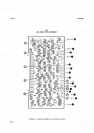
Use an oscilloscope along the signal path to locate a dead stage.
Check the dc levels along the signal path. Beginning after stage two, the dc level alternates between
-
0.7V and
OV with each successive stage because of the direct coupling of the stages. This is noted in the waveforms
indicated on the schematic.
Log
Fidelity Accuracy:
Begin testing by establishing a top graticule reference (eighth graticule). Reduce the
input signal level in 10 dB steps and observe the variations between each step. Now, establish a reference at the
next graticule
100
mV lower (seventh graticule). Step the signal level again and observe the variation between the
steps. Continue lowering the reference point until each step below the reference point is within specification.
This will indicate at which step the inaccuracies are being introduced. If the error occurs between the 800
mV
reference and the 700 mV reference, the problem is probably in the first stage. If the problem is present at
all
reference levels except the last one, the problem is probably in the last amplifier stage, since it compresses first.
The most probable causes of failure are PIN diodes, Schottky diodes, transistors, capacitors, and resistors, in
that order.
Schottky diodes have a dc resistance of about
300
to 330 ohms. The value varies, depending on the current
supplied by the ohmmeter. The values should, however,
all
be within 10% of each other.