


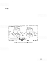


MODEL 8559A SERVICE
STEP GAIN ASSEMBLY A12, CIRCUIT DESCRIPTION
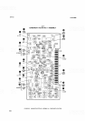
The Step Gain Assembly A12 provides from 0 to 50 dB amplification of the 21.4
MHz
IF in 10 dB steps, as
selected from the REFERENCE LEVEL control. A zero to
-
12 dB REFERENCE LEVEL FINE attenuator
control is also included on the front panel. Generated on the Step Gain Assembly A12 are the first mixer diode
bias and a flatness control voltage proportional to the sweep plus tune (S
+
T) voltage.
Step Gain Amplifiers (E)
(F)
(G)
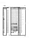
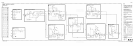
There are three step gain amplifiers, one 10 dB and two 20 dB, cascaded as shown in the schematic diagram.
Full gain of any amplifier is selected by grounding the appropriate IFG line. The three step gain amplifiers can
be considered as operational amplifiers.
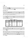
An
equivalent circuit for the three stages is shown in Figure 8
-
57. The
gain for each amplifier is: Gain
=
1
+
R,/R,. The feedback resistance, R,, for the 10 dB amplifier is R8, 562
ohms; for the 20 dB amplifiers it is
R23
and R31, each 750 ohms. The input resistance,
R,,
is a combination of a
fixed series resistance (56.2 ohms) and the controlled resistance of the PIN diodes. The resistance of the PIN
diodes is approximately 10 to
1000 ohms and increases as the forward bias current is decreased from 100
milliamperes to
1
microampere. The input resistance,
R,,
for the 10 dB amplifier is approximately 260 ohms; for
the 20 dB amplifiers, it is about 83 ohms.
FIGURE
8
-
57.
STEPGAIN AMPLIFIERS, SIMPLIFIED DIAGRAM
Selection of the correct combination of step gain amplifiers is accomplished with the REFERENCE LEVEL
switch. Rotating the switch grounds the emitter circuit of the selected amplifier (or amplifiers), allowing current
to flow through the PIN
di8de (or diodes). The possible switch combinations allow the gain to vary from unity
(all switches open) to 50 dB maximum with all three emitter circuits grounded.
TestINorm Switch.
In the emitter paths of the 20 dB step gain amplifiers are the TEST/NORM switches
used to disable both 20 dB amplifiers during log amplifier adjustment.
0-12dBControl
(H)
The REFERENCE LEVEL FINE control provides approximately 0.3 to 12.3 dB of attenuation at the base of
46 in the
0
-
12 dB control circuit. By regulating the current flow through PIN diode CR7, the amount of signal
attenuation is controlled. For example, if PIN diode current flow is increased, more
RF
signal is shunted or
bypassed to ground. Capacitor C23 provides the RF ground path.
A minimum current flow through the PIN diode, which provides the maximum allowable diode resistance, is
established by
-
12 dB potentiometer R39 so that the diode is never completely cut off. Adjustment of R39 sets
the 0.3 dB point and is adjusted with the REFERENCE LEVEL FINE control set fully clockwise
(
-
12 posi
-
tion).
8143