


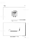

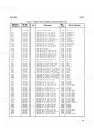
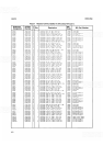

SERVICE
MODEL
8559A
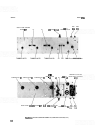
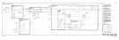
Resistor R92 is an adjustable current limiter that makes possible sweep width adjustment by changing the gain
of the stage. Delay compensation for FM coil swept spans is provided by U14, C14,
R96*, and potentiometer
R83, the delay compensation adjustment.
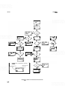
YTO Main Coil Fixed Driver
(F)
This driver supplies current to the YTO main coil to set the start frequency of the first LO WIG-Tuned Oscilla
-
tor Assembly A6) at approximately 3 GHz. Resistor R8 adjusts this frequency by changing the reference voltage
at U3 and, therefore, the drive to
Q5. MOSFET Q5 buffers the operational amplifier's output and supplies
current drive to the YTO main coil.
Alternate IF Driver (YTO) (C)
A voltage divider, R18 and R19, form a nominal
+
5V source that supplies U7 and establishes pull
-
up voltages
on the H2, H3, and PM lines. When alternate IF is selected, current to the YTO main coil changes, shifting the
sweep
-
center frequencies by
+
15 MHz/N, where
N
is the harmonic number associated with the selected band.
Four
-
to
-
ten
-
line decoder U4 decodes front panel band information and activates the appropriate section of U1.
This selects the resistor that is paralleled with R9 in the YTO Main Coil Fixed Driver. Altering the effective
resistance of R9 changes the current drive to the YTO main coil by changing the gain of the YTO Main Coil
Driver circuit.
YTO Main Coil Filter
(E)
When FM coil spans (<1 MHz/div) are selected, A16Q1 connects A16C22 (both located on the motherboard)
-
across the main coil of the YTO to filter noise and line related signals. During wide spans (>1 MHz/div), the
charge on
A16C22 is maintained by US, Q1, 43, and associated circuitry. Diodes CR3 and VR1 protect the
filter from excessive back EMF (electromotive force) generated by the YTO.
Voltage Regulators (H) (I)
(K)
Precision, temperature compensated, Zener diode VR2 provides the reference for the voltage regulators. The
output of the
+
14.5V supply is fed back through R39 to bias VR2, while VR3 ensures that VR2 initially turns
on. Transistor
44 is a series pass element driven by U6 and Q5, while R35, R40, and R41 sample the output
voltage and provide adjustment.
The
-
12V supply tracks the
+
14.5V supply and consists of a pass element, 47, driven by U8.
The
-
10V regulator supplies the voltage to the TUNING control, and is heavily filtered by C3 and R33.
Transistor
46 is the series pass element driven by U7 and resistor R29 adjusts the output voltage level.
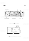
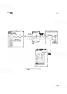
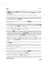
FREQUENCY CONTROL ASSEMBLY A7, TROUBLESHOOTING
The Frequency Control Assembly A7 is the principal cause of excessive residual FM of the YIG
-
Tuned Oscilla
-
tor's output. The following are a series of tests to help isolate the source of FM to a function block on the
Frequency Control Assembly. Components most likely to be the source of the FM in each block are also listed.
Be sure to check the following power supply voltages, for correct level and excessive ripple, before proceeding:
the
+
14.5V Regulator (block H), the
-
10V Regulator (block I), the
-
12V Regulator (block
K),
and the
+
15V
and
-
12.6V Power Supplies (block
J).