


SERVICE MODEL 8559A
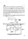
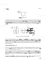
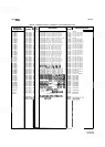
The case capacitance of the crystal (C,) would cause a second resonant point, or dip,
in
the bandpass
if
compensation were not used to nullify its effects. Compensation is provided by 44 as a current equal to and
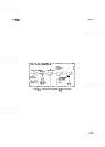
opposite in phase with the current flowing through C,, as shown in Figure 8-51. Capacitor C15 (SYM) adjusts
the phase of the compensating current.
TOIFROM
10
dB
INPUT
BUFFER AMP
T
0
UNITY GAIN
BUFFER AMP
FIGURE8-51. COMPENSATION AMPLIFIER
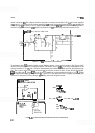
The input capacitance of the unity gain buffer, the trace capacitances, and the capacitance of the PIN diode
add, causing the center frequency of the filter to be altered. Compensation is used to eliminate this effect. These
capacitances are tuned out by including them in a parallel resonant circuit (at 21.4 MHz) formed with L7 and
fine tuned by C25 (CTR). Adjusting C25 tunes the circuit to present a high impedance at resonance.
When LC filtering is selected,
BW5F forward biases CR2, effectively grounding the emitter of 43. During
crystal filtering,
CR2 is reverse biased.
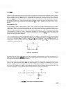
First
LC
Pole
(C)
LC filtering is used for bandwidths of 100 kHz, 300 kHz, 1 MHz, and 3 MHz. The relationship of an individual
pole's bandwidth to the selected bandwidth is the same as the crystal pole's
(2.3
times per pole and 1.5 times per
assembly). The LC filter pole comprises a metallized inductor (L6) in parallel with four capacitors: the series
combination of
C16* and C20*, C21 (temperature compensation), and C23 (center adjust). This resonant
circuit is driven through
CR3, which functions as a variable resistor. Bandwidth control line BW7F establishes
the current through CR3 and thereby controls the pole's bandwidth. Feedback from the unity gain buffer
replenishes losses in the resonant circuit.
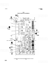
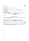
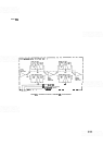
A simplified model of the LC pole is shown in Figure 8-52. At resonance, a voltage divider is formed between
CR3 and the resonant circuit. The 3 dB points of the
bandpass occur when the PIN resistance and the impe
-
dance of the resonant circuit are equal. Varying the PIN resistance varies the filter's 3 dB points. The higher the
PIN resistance, the narrower the bandwidth. When the 100 kHz bandwidth is selected, CR3 is reverse biased
and
R19* sets the bandwidth; if one of the other bandwidths is selected, the parallel combination of R19* and
CR3 is utilized. The intrinsic capacitance of PIN diode CR3 affects the bandpass, if not compensated for.
Adjustable capacitance C73 (LC DIP) and L5 are in parallel with the PIN capacitance and allow it to be tuned
out of the circuit.