


SERVICE
MODEL8559A
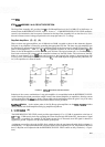
The maximum current flow through the PIN diode is set with the 0 dB potentiometer R35. Resistor R35 is
adjusted to the 12.3 dB attenuation point with the REFERENCE LEVEL FINE control set fully counterclock
-
wise (0 position).
Transistors Q5 and
47 are identical current sources. The maximum current is set with the
0
dB adjustment, R35,
in the common base circuit. Diode CR5 provides temperature compensation for the transistors.
Transistor
Q5 provides current for a bias voltage applied to the anode of the PIN diode. The voltage source
consists of R39, R38, and CR6. Diode CR6 provides temperature compensation for the PIN diode. Inductor
L8 isolates the diode current source from the RF signal.
Transistor
47 provides current for a variable voltage source at the cathode of PIN diode CR7. Fixed resistor
R40 is effectively in parallel with the negative side
(
-
12.6V) of the REFERENCE LEVEL FINE control
potentiometer. Its purpose is to match the FINE control to changes in the PIN diode resistance. The FINE
control varies the voltage at the PIN diode cathode, this varies the diode current flow. When the FINE control
is fully clockwise, the PIN diode is at minimum conduction and maximum signal is applied to the base of
46.
Conversely, when the FINE control is fully counterclockwise, the PIN diode is forward biased into maximum
conduction and minimum signal is applied to
46. Buffer amplifier 46 operates as an emitter follower, providing
isolation between the 0
-
12 dB control circuit and the 21.4 MHz bandpass filter.
21.4
MHz
Bandpass Filter (I)
The 21.4 MHz Bandpass Filter at the output of the
0
-
12 dB control circuit is a two
-
pole type used to reduce the
out
-
of
-
band noise produced by the step gain amplifiers and 0
-
12 dB control.
NOTE
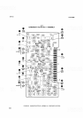
For minimum step gain error, the ground plane on the Step Gain Assembly
A12 must be firmly connected to the chassis extrusion and the Motherboard
Assembly A16 common ground. This means that before you can make any
step gain measurements or adjustments, the Step Gain Assembly A12 must
be fully seated in its connector socket and all of its cover screws must be in
place and tightened. You can, however, leave the gold secondary cover off
for these measurements.
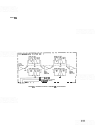
Band Select Decoder (A)
Band select decoder U3 is a 4
-
to
-
10 line decoder. It decodes the three band
-
select lines (H2, H3, and PM) to
select one of six output lines. The selected line goes low while the remaining five lines stay high. The status of the
decoder's outputs controls the tilt, offset, and bias circuits.
Band Tilt
(C)
Band tilt is controlled with a variable, voltage
-
controlled voltage source comprising operational amplifier U4b,
current boosting transistor 42, and related adjustable resistor networks. The signal input to this circuit is the
sweep plus tune
(S
+
T)
voltage. Normally, this signal is a ramp extending from
+
1.2V to
+
4.8V or some level
in between, depending on the position of the FREQ
SPAN/DIV and frequency TUNING controls.
When the
S
+
T ramp is at its low point
(+
1.2V), the level at test point 3 should be
+
10.6V
+
0.1V When the
S
+
T ramp is at its peak
(+
4.8V),
the level at test point 3 can be adjusted from about
+
9.6V to
+
10.9V with
the circuits's potentiometers and factory selected fixed resistors. Potentiometers R47, R48, R49,
R51, R53, and
R55 adjust the overall tilt for each band. Ttvo factory selected resistors, R5O and R52, and potentiometers R54
and R56 provide additional tilt adjustment for harmonic mixing bands 2
+
,
2
-
,
3
+
,
and 3
-
after a break
-
point at approximately midband.