


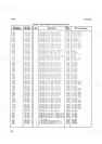


SERVICE
MODEL
8559A
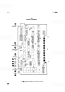
AMPL
l
F
l
ER
=
t1OV
RETRACE
=
+0.5V
SWEEP
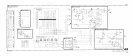
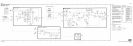
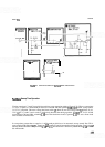
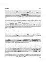
FIGURE
8
-
34.
SIMPLIFIED SCHEMATIC OF SWEEP GENERATOR IN AUTO MODE
With CR2 off, the current source begins charging the timing capacitor (C3 and C4, block
I).
As the timing
capacitor charges, the output of the buffer amplifier increases linearly. Transistor 433 is on and its collector
voltage is about
+
0.5Y
The voltage at U1 pin 2 is mainly established by sweep voltage divider R29, R39, and
R47*. (Components VR1, CR4, and R40 feed back some of the comparator's output to pin 2 and act upon the
divider. These components have been omitted to simplify the model; see block
L
on the main schematic.)
When the ramp voltage reaches
+
5V, the U1 pin 2 is approximately
+
2.78V. Consequently, the comparator's
output swings to about
-
4V. This negative change reverse biases CR6 and turns 433 off. Resistors R42*, R39,
and R29 form a divider that, when combined with the feedback loop and the buffer amplifier, sets the ramp
voltage at
-
5V during the dead time. (Factory selected resistor R42* adjusts the dead time voltage.)
The timing capacitor is discharged by the comparator and quickly reaches
-
5V. The ramp remains at
-
5V until
the dead time capacitor charges to
+
1.2V and the sweep cycle is repeated.
Other components in the sweep generator have the following functions: Capacitor C6 speeds up the switching of
U1. Capacitor C8 and resistor R33 desensitize U1 from power spikes. Frequency compensation for U1 is
provided by C9, feedback compensation by C7. Zener diode
VR1, switching diode CR4, and resistor R40 bring
U1 out of saturation at the end of the ramp to improve switching time.
&98