


BERT Technical Articles
B-28 GB1400 User Manual
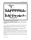
To stress the noise margin, the PRBS spectrum must have components below the coupling circuit’s cutoff
frequency, f
L
. For example, a 23-stage PRBS generator with a bit rate, f
c
, of 44.7 Mbits/s has a pattern
length of 2
23
-1=8,388,607 bits.
The fundamental frequency, f
F
, is f
c
/8,388,607=5.33 Hz. If f
L
=32 kHz, thousands of the pattern’s spectral
components are removed. The fraction of power removed is given by πfL/fc, and the square root of that
figure is the rms error as a fraction of the signal level:
rms error = πf
L
/f
c
= 0.047
This error appears as Gaussian noise with an rms value that is 4.7% of the noise margin. The more
spectral components below the cutoff frequency, the more Gaussian the noise is. However, if fundamental
would be the PRBS pattern length was 27-1, the 350 kHz, which is greater than f
L
. The noise margin
wouldn’t be stressed, and the formula for rms error wouldn’t hold.
Similarly, a PRBS pattern will stress the clock-recovery circuit if the pattern’s fundamental is within the
B
. If it is, the pattern introduces random fitter in the recovered clock. The jitter’s
magnitude depends on f
B
and on offsets within the circuit. The rms jitter is not a function of the PRBS
pattern length, but the peak jitter increases with pattern length.
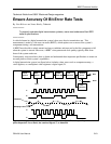
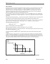
Examining Jitter
An important factor in a data transmission system is jitter. Ideally, all clock and data signals in the
systems have a constant frequency with no phase modulation. In practice, a clock source has some phase
modulation, or jitter, and noise and imperfect equalization introduce additional jitter. The following
discussion examines clock-source jitter alone, assuming that noise and distortion contribute no jitter.
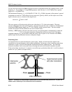
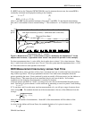
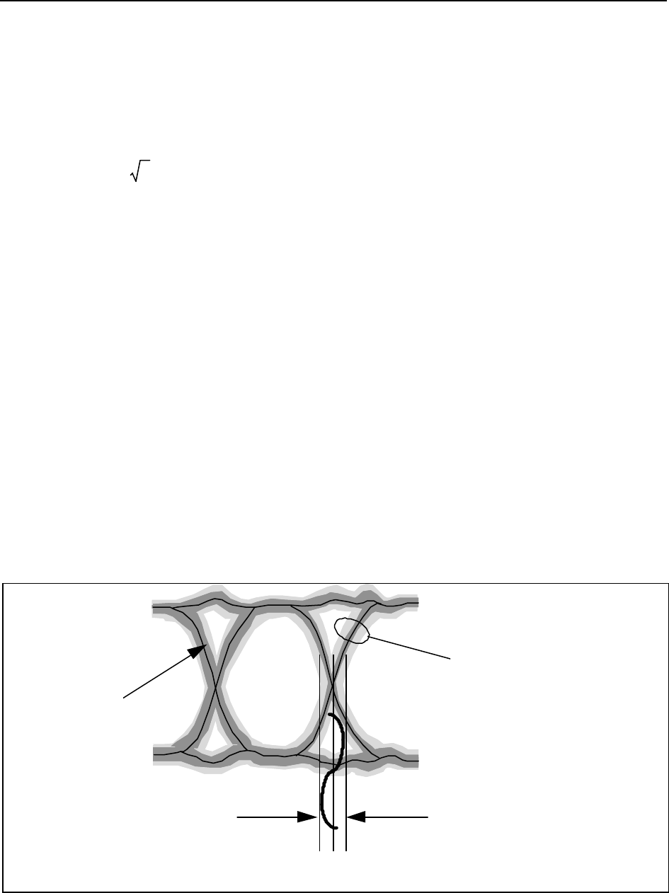
If the received data waveform, F, is viewed on an oscilloscope synchronized data, the 1s and 0s overlap to
produce an “eye” pattern (see figure below).
+ Peak- Peak
Ideal pulse
position
Jitter modulation
Superimposed pulses
with jitter modulation
Figure 4. Viewed on an oscilloscope synchronized to the received data, phase error, or jitter, θθ
e
shows up as a widening of the recovered clock's waveform.