


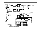

Theory of Operation
I-2 GB1400 User Manual
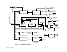
The Error Inject circuitry consists of a chain of decade counters, used to generate
a pulse every 10E-n bits (where n=3-7). This pulse generates a single bit error on
the output data streams, providing a known error rate for back-to-back tests.
Data and Clock Output Amplifier PCB
The Data stream generated on the Data Generator PCB is sent to the Output Amp
PCB, relatched into a flip flop, and differentially driven into a monolithic GaAs
pulse amplifier which drives the front panel DATA and DATA invert outputs.
The amplifier provides adjustment, controlled by DACs, of the Data output
Amplitude and baseline Offset. The amplifier will drive 2 Volts peak-to-peak
into a 50 Ohm load, unterminated 4 Volts peak-to-peak, suitable for Fast TTL
and CMOS.
The System Clock signal is sent to the Output Amp PCB, distributed to the Data
latch and also to a discrete GaAs FET pulse amplifier which drives the front
panel CLOCK and CLOCK invert outputs. The amplifier provides adjustment,
controlled by DACs, of the Data output Amplitude and baseline Offset. The
amplifier will drive 2 Volts peak-to-peak into a 50 Ohm load, unterminated 4
Volts peak-to-peak, suitable for Fast TTL and CMOS.